Octek was a motherboard manufacturer for the IBM PC and its compatibles during the DOS era. They also made the odd peripheral card too, including graphics cards.
Their 286 motherboards in particular are well-known in the retro PC community for being robust and, with their use of Headland chipsets, pretty fast.
They were acquired by Ocean Information Systems, Inc. around 1996.
Ocean Office Automation Ltd. (OCTEK)'s head office address is at
5/F., Kader Ind. Bldg.,
22 Kai Cheng Rd.,
Kowloon Bay, Kowloon, H.K.
Tel: (852) 2305 1800,
Fax: (852) 2799 2298,
website: http://www.oceanhk.com
In the US, their head office address is USA California
Ocean Information Systems Inc., 688 Arrow Grand Circle,
Covina, California 91722, USA,
Tel: (818) 339-8888,
Fax: (818) 859-7668, website: http://www.ocean-usa.com/ocean
Fox II 286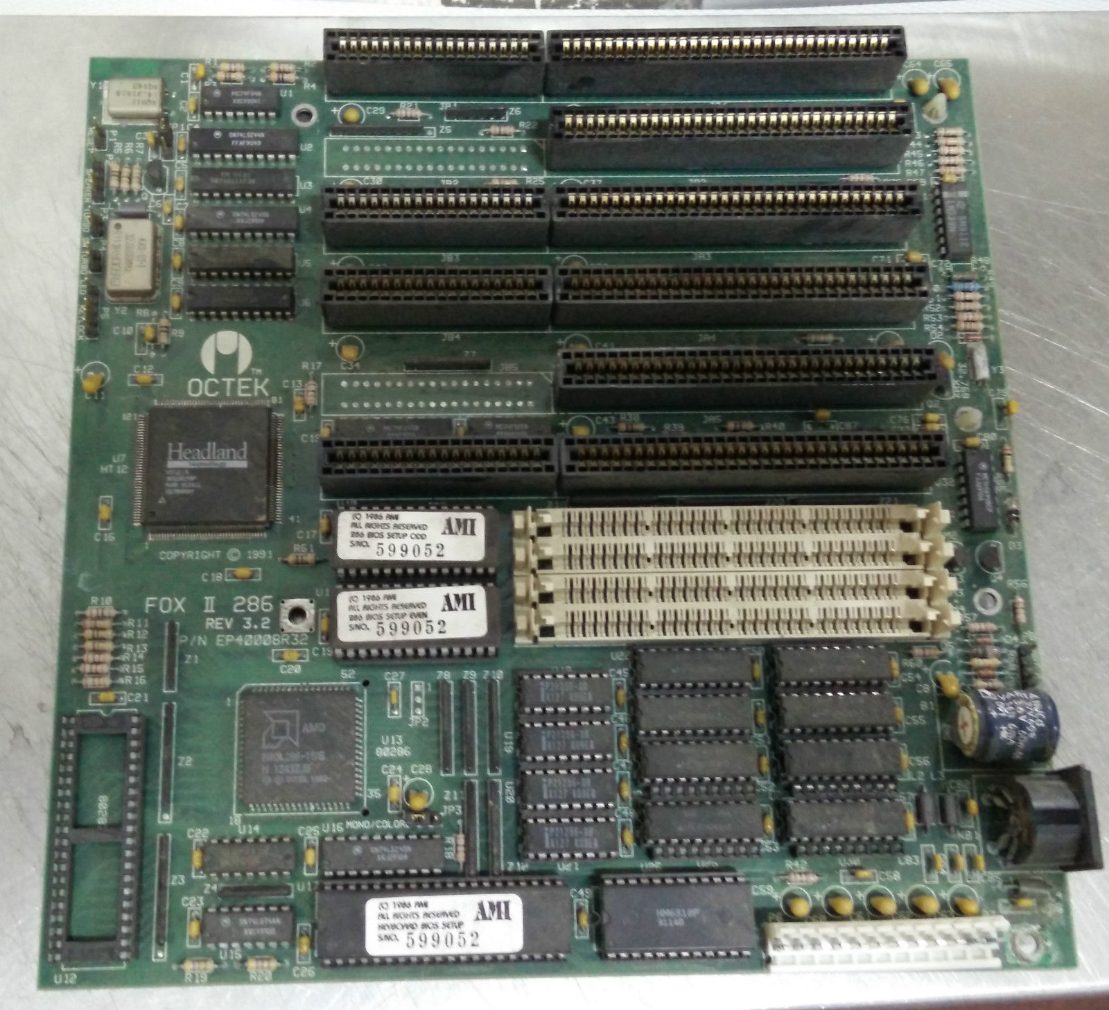
Year: 1991
Type: 80286
Form Factor: Baby AT
Power Connector: AT
Chipset: Headland HT11
BIOS: American Megatrends
Slots: 4 x 16-bit ISA, 2 x 8-bit ISA
Memory: 8 x 30-pin SIMM
Known Board Revisions: 3.2
BIOS Strings:
DH1X-6069-113090-KF
Fox II is another 286 board that employs the single-chip Headland HT1x chipset. It supports 80286 CPUs of 16 MHz.
Note that some board revisions (3.2) have soldered-in 80286 CPUs rather than a CPU socket. |
Fox M 286
Year: 199x
Type: 80286
Form Factor: Baby AT
Power Connector: AT
Chipset: Headland HT1x
BIOS: American Megatrends
Slots: 4 x 16-bit ISA, 2 x 8-bit ISA
Memory: DRAM ICs
Known Board Revisions:
BIOS Strings:
Fox M is a very modern, compact 286 board that employs the single-chip Headland HT1x chipset. It supports 80286 CPUs of up to 25 MHz!
This board is fascinating to me, as it would be a good contender for a retro PC build to compete against the early 386 era. The |
Pony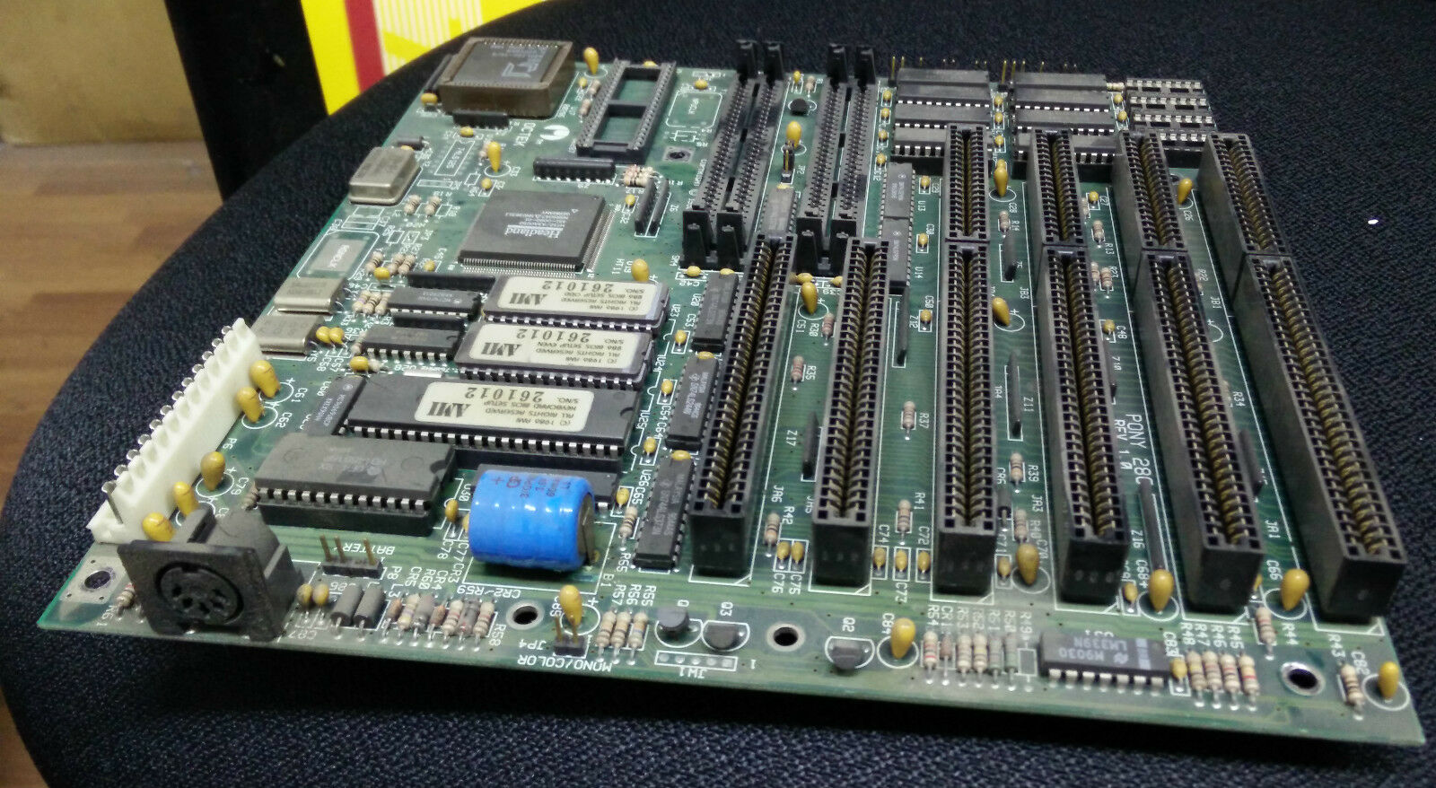
Year: 1990
Type: 80286
Form Factor: Baby AT
Power Connector: AT
Chipset: Headland HT12(?)
BIOS: American Megatrends
Slots: 4 x 16-bit ISA, 2 x 8-bit ISA
Memory: 4 x 30-pin SIMM
Known Board Revisions: 1.0
BIOS Strings:
This Pony is a single-chip HT1x chipset board with a socketed 80286 CPU. It supports 2 banks of 30-pin SIMMs. |
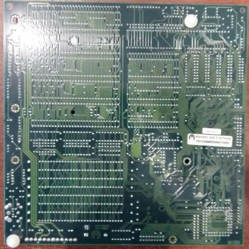
Jaguar
Year: 199x
Type: 80386
Form Factor: Baby AT
Power Connector: AT
Chipset: Macronix 83C305/306
BIOS: ?
Slots: 4 x 16-bit ISA, 2 x 8-bit ISA
Memory: 8 x 30-pin SIMM
Known Board Revisions: ?
BIOS Strings:
The Macronix 83C305/83C306 chipset contains a built-in 8 KB level 1 cache.
More Images
|
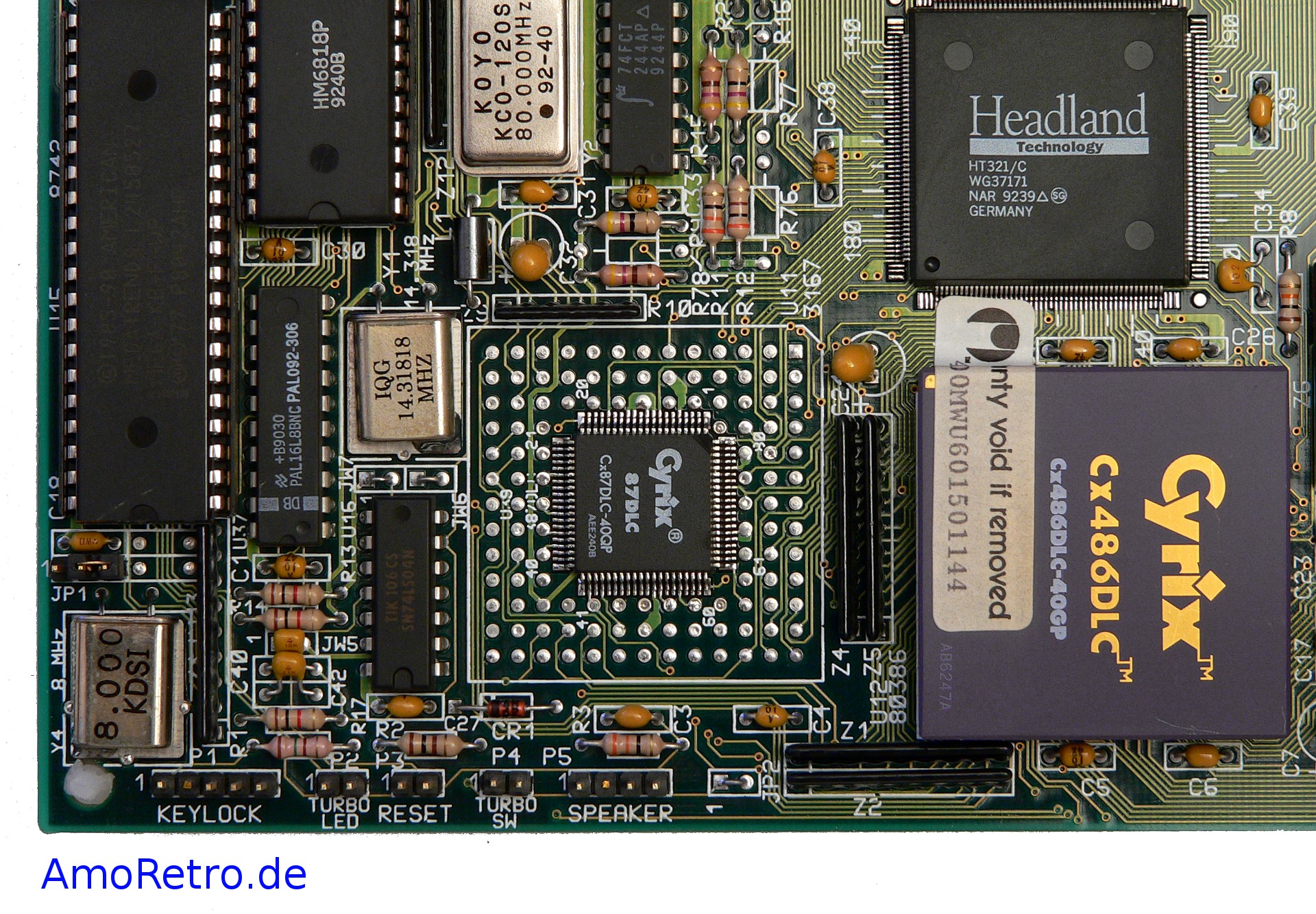
Jaguar IV-P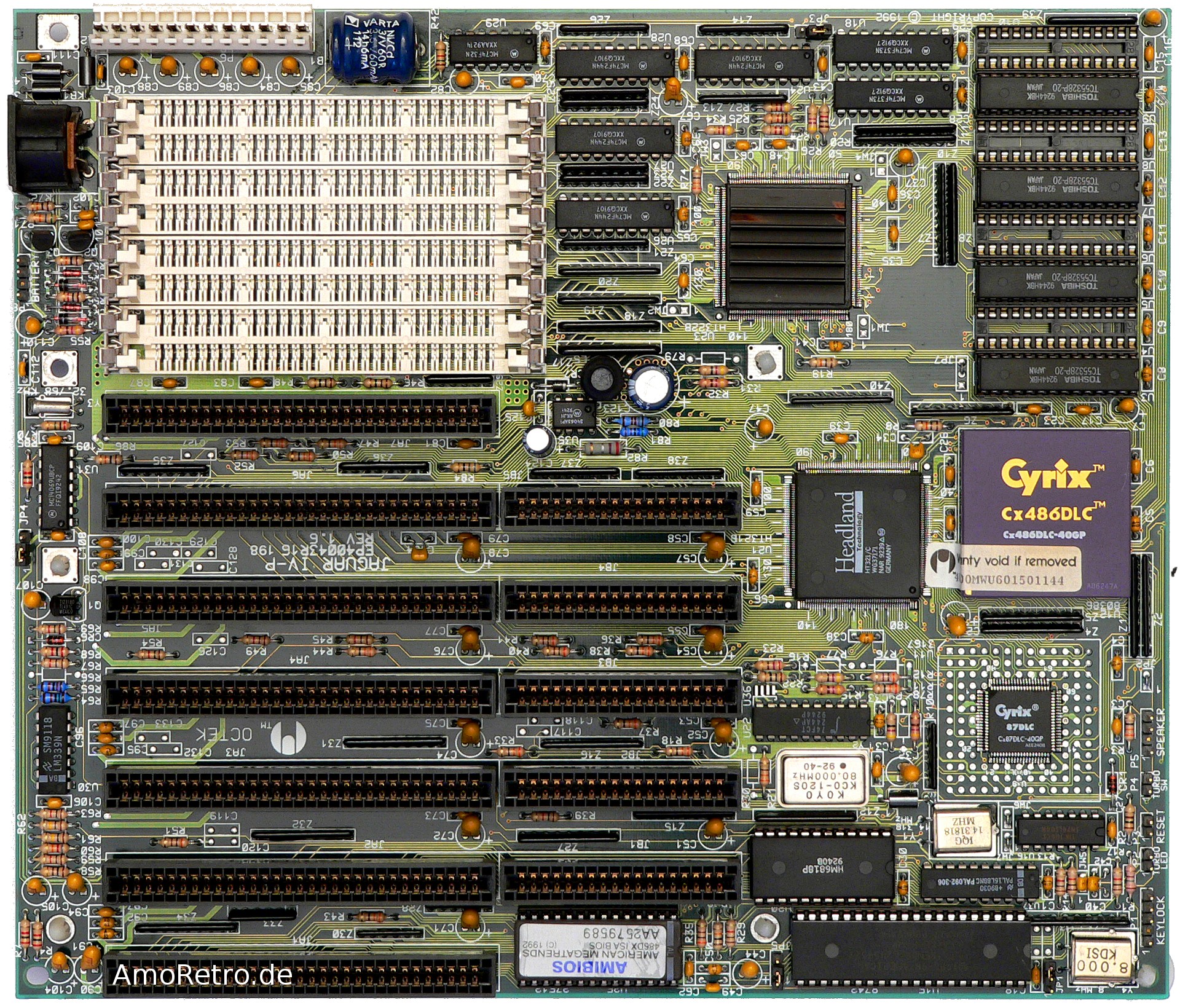
Year: 1992
Type: 80386 / 486
Form Factor: Baby AT
Power Connector: AT
Chipset: Headland HT321/C
BIOS: American Megatrends
Slots: 5 x 16-bit ISA, 2 x 8-bit ISA
Memory: 8 x 30-pin SIMM
Known Board Revisions: 1.6
BIOS Strings:
More Images
|
 Panther II Panther II
Year: 199x
Type: 80386SX
Form Factor: Baby AT
Power Connector: AT
Chipset:
BIOS: ?
Slots: ?
Memory: ?
Known Board Revisions: ?
BIOS Strings:
More Images
User Manual |
Hippo 12 VIP / Hippo-12 / Hippo-12
Year: 199x
Type: Socket 3
Form Factor: Baby AT (8.5" x 11")
Power Connector: AT
Chipset: UMC 8881/8886 PCI
BIOS: Award
Slots: 4 x 16-bit ISA, 2 x VESA Local Bus, 3 x PCI
Memory: 4 x 72-pin SIMM (4 MB up to 256 MB)
Known Board Revisions: ?
BIOS Strings:
Supports Intel 486SX/DX/DX2/DX4 up to 100 MHz, AMD 486DX/DX2/DX4 up to 120 MHz, AMD X-5 5x86-133, Cyrix 486DX/DX2/DX4 up to 100 MHz, and Cyrix 5x86 100 and 120 MHz. Onboard 3.3V voltage regulator.
Level 2 cache is 256 KB as standard, but also supports 0 KB, 64 KB, 128 KB and 512 KB.
Main memory supports 4 MB, 8 MB, 16 MB, 32 MB and 64 MB modules (x32 or x36).
Onboard EIDE via the UMC 8004 PCI EIDE chipset, supporting up to four Mode 3 and Mode 4 drives.
Jumper Settings:
CPU Type
TYPE      JP1 JP2 JP18 JP19 JP20 JP24 JP25 JP26 JP30 JP31 JP32 JP34 JP35 JP36 JP37
-----------------------------------------------------------------------------------
Intel 	   1-2 1-2 1-2  3-4  open open open open 1-2  open open open open open open
486DX/DX2	   3-4
Intel 	   1-2 1-2 2-3  open open open open open 1-2  open open open open open open
486SX
Intel 	   1-2 1-2 1-2  2-3  open 2-3  1-2  open 3-4  open 2-3  2-3  1-2  2-3  open
P24T	   	   3-4            4-5            5-6
Cyrix 	   2-3 1-2 2-3  open open 1-2  2-3  open 3-4  open 2-3  1-2  2-3  1-2  open
CX486S                           3-4
Cyrix 	   2-3 1-2 1-2  3-4  open 1-2  2-3  open 3-4  open 2-3  1-2  2-3  1-2  open
CX486D            3-4            3-4
UMC-U5S   1-2 2-3 2-3  1-2  open open 3-4  open 1-2  open 1-2  open open open open
                       3-4
Intel 	   1-2 1-2 2-3  open open 2-3  open open 3-4  open 2-3  2-3  open open open
SL 486SX                         4-5
Intel SL  1-2 1-2 1-2  3-4  open 2-3  open open 3-4  open 2-3  2-3  open open open
DX/DX2/DX4        3-4            4-5
AM486DXL  1-2 2-3 1-2  1-2  open open 3-4  open 1-2  open 1-2  open open open open
AM486DX4          3-4  3-4
UMC-U5DS
AM486DX2  1-2 1-2 1-2  3-4  open 2-3  open open 3-4  open 2-3  2-3  open open open
AM486DX4          3-4            4-5
P24D      1-2 1-2 1-2  3-4  2-3  2-3  open 1-2  3-4  1-2  2-3  2-3  open open 1-2
                  3-4            4-5
AM486DX2  1-2 2-3 1-2  1-2  1-2  open 3-4  open 1-2  open 1-2  open open open open
                  3-4  3-4
AMD       1-2 1-2 1-2  3-4  2-3  2-3  open 1-2  3-4  1-2  2-3  2-3  open open 1-2
5X86-133          3-4            4-5
Cyrix5x86 1-2 1-2 1-2  3-4  open 2-3  open 1-2  3-4  1-2  2-3  2-3  open open open
                  3-4            4-5

Remark:
-------
To support AMD 5X86-133 CPU:   BIOS Rev.095-036 (Sept 26, 1995) is required and JP33 = 2-3.
To support Cyrix 5x86-100 CPU: BIOS Rev.095-036 (Sept 26, 1995) is required and JP33 = open.
CPU Clock Multiple
JP33	Intel 486DX4 / AMD Enhance 486DX4
--------------------------------------------------------------------------------
open	CLK 3x
1-2	CLK 2.5x
2-3	CLK 2x

Clock Selection
JP16            Clock Rate      CPU speed
--------------------------------------------------------------------------------
1-2             50MHz           DX50
1-2,3-4,5-6     33MHz           DX33, DX2-66, DX4-100
3-4,5-6         40MHz           DX40, DX2-80
5-6             25MHz           DX25, DX2-50

CPU Voltage
TYPE    CPU VCC        JP41	JP42	JP43	JP44	JP45	JP46
--------------------------------------------------------------------------------
AUTO	5V/3.45V        open	open 	open	open	1-2     open
FIXED	5V              open	open 	open	open	open    1-2
FIXED	4V              open	open 	open	1-2	    open    open
FIXED	3.8V            open	open 	1-2	    open 	open    open
FIXED	3.6V            open	1-2 	open	open	open    open
FIXED	3.45V           open	open 	open	open	open    open
FIXED	3.3V            1-2	    open 	open	open	open    open

Cache Configuration
For 33MHz clock, the tag RAM 32Kx8 is used 20ns, and 40MHz or 50MHz system, 15ns RAM is used (U10).
       512K            256K            256K            128K
       128Kx8          32Kx8           64Kx8           32Kx8
      U1,U3,U6,U8     U1-U4,U6-U9     U1,U3,U6,U8     U1,U3,U6,U8
-------------------------------------------------------------------------------
JP5	2-3             1-2             2-3             2-3
JP14	1-2,3-4         1-2             1-2             open

On-board IDE
JP11	IDE
-------------------------------------------------------------------------------
1-2	enabled
2-3	disabled

Slot Configuration
JP39
-------------------------------------------------------------------------------
Close	VL slot clock greater than 33.333MHz
Open	VL slot clock less than or equal to 33.333MHz

JP40
-------------------------------------------------------------------------------
Close	1 WS VL-write cycle
Open	0 WS vl-write cycle
|
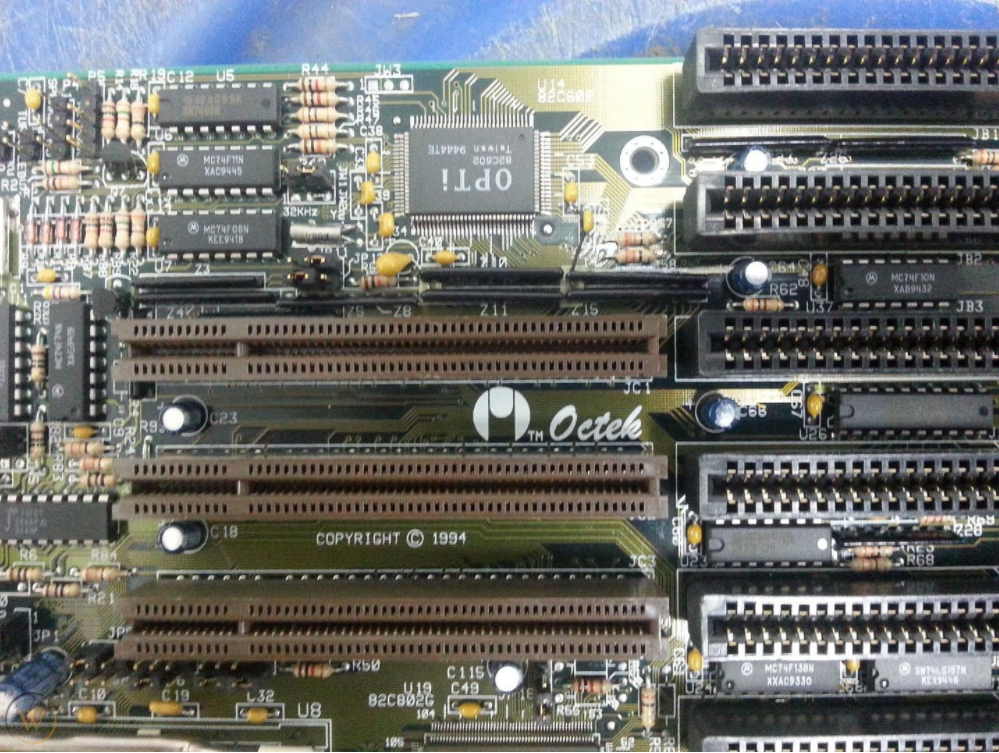
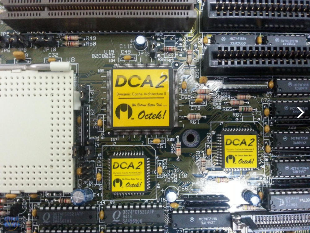
Hippo VL+ DCA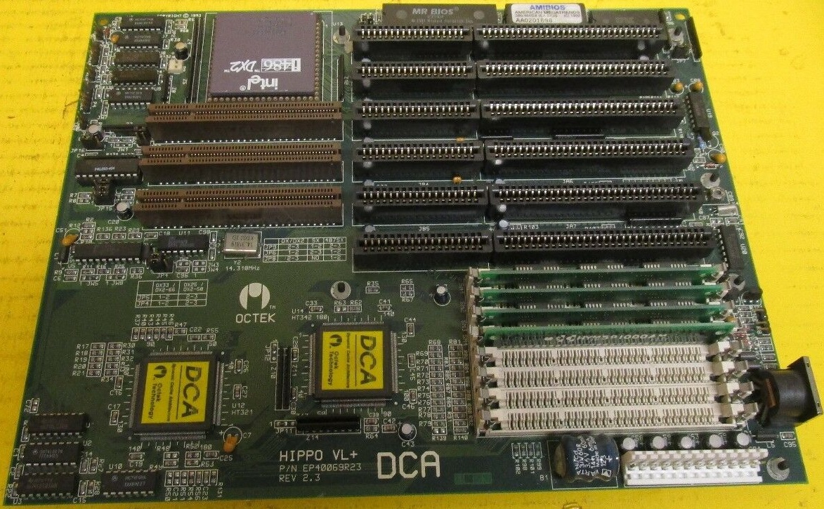 / DCA1 / DCA1
Year: 1994
Type: Socket 3
Form Factor: Baby AT (8.5" x 11")
Power Connector: AT
Chipset: Headland HTK340
BIOS: MR (Microid Research) or AMI
Slots: 6 x 16-bit ISA, 3 x VESA Local Bus
Memory: 8 x 30-pin SIMM (64 MB maximum)
Known Board Revisions: 1.1, 2.3
BIOS Strings:
Supports Intel 486SX-33, 486DX-33, DX2-66, DX4-100, and P24T. From AMD, DX2-66 and DX4-100, and from Cyrix, DX2-66, DX4-100 and 5x86-100.
The DCA1's L2 cache is called Dynamic Cache Architecture (DCA) Level 1:
" D.C.A. Dynamic Cache Architecture
The Future of Memory Cache Operations Standards
Ocean is proud to announce the End of External Cache in 486 Based Systems !
External Cache has been, for years, the industry standard for enhancing the performance between the Random Access Memory (RAM) and the 80486 CPU. These Static RAM configurations, usually 64K to 512K Bytes have provided motherboard manufacturers a convenient, though expensive, solution to caching system RAM.
The major drawbacks to external cache are:
- The cost of SRAM chips and of DRAM sockets.
- The additional manufacturing costs associated with the additional hardware.
- The large percentage of System Clock Time used in a Write Back Operation.
(Usually 75% or more of the total cache operation time)
- The additional set up requiring board level jumpers and CMOS settings.
- The reliability problems associated with the numerical high speed components (SRAM).
Ocean is now offering a 80486 based motherboard, utilizing a revolutionary technology that enhances the performance of the internal cache now offered in 80486 CPUs. Dynamic Cache Architecture, DCA, introduces a "Byte Gathering Write Buffer". Very simply, most software, including Novell Netware, and Microsoft Windows, is written for 386 based systems. This means that regardless of what kind motherboard is being used, information is transferred only in 8 and 16 bit "Packets". This is due to the BUS limitations (16 bits wide) of 386 based systems. A 486 system, until now, moved information in the same manner because the software written to take full advantage of the 486's 32 bit wide BUS has usually been restricted to CAD/CAM, Expert Systems, Virtual Simulations and other High End applications. The Byte Gathering Write Buffer collects the 8 and 16 bit "packets" of information until a single 32 bit "packet" is formed then " Writes" this single informational "string" back to RAM in one operation, rather than in several time consuming ones. This is a tremendous improvement on the efficiency of data transfer, as the information is handled solely through the CPU, the High Speed Chipset and the lightning fast Internal Cache of the 80486. The performance scale for our Hippo IV 486-25/33 is simple: Equal or greater performance for less money!"
Octek website, February 1998
Memory support is via 4 banks of 72-pin modules of 4 MB or 16 MB capacity. 'x32' SIMMs are supported.
With its VESA Local Bus, up to 33 MHz bus speeds are possible.
The DCA1 comes with an onboard 5V/3.3V voltage regulator for 3.3V CPUs, an OverDrive socket for Pentium Technology processors, and onboard 'POWERGOOD' generation.
" DCA Cache Architecture 486 PC surpasses performance of other secondary cache 486 PC's by virtue of a smartly designed unary cache system and support for higher performance processors. DCA's internal multibyte gathering write cache technology fully optimize memory cycles, achieving up to 4 times better performance in CPU data WRITE transfers compared to other complex cache systems.
Dynamic Cache Architecture
Ocean
Information Systems, Inc.
Testing Procedures:
When testing a DCA based motherboard with several of the most popular shareware or freeware benchmarks, you may encounter some unusual results. Some may be outstanding to the point of disbelief and other may show mediocre scores. The following explanation was compiled to help clarify the performance testing of DCA.
DCA is architecturally different than External Cache:
DCA is a completely new and different way of handling cached instructions and data. The main design focus of DCA was on what was done with cached instructions AFTER they had been processed. It was found that most of the time spent during a cache cycle was spent in the cache WRITES and cache MISSES. DCA addresses these specific areas with technology that until now was used exclusively in the Mainframe Computer. These include the four level deep 32 bit wide byte gathering buffers, burst mode 32 bit writes to RAM and quad instruction piplining at the chipset level. The DCA Byte Gathering Buffers are also READ/WRITEable, meaning that instructions and/or data that is redundant or is called repetitively need not be transferred to RAM before it is executed again. It can be read to, written from or altered directly from DCA without additional clock cycles being wasted. This also reduces cache misses (internal) by almost 98%. For every cache HIT there must be at least one cache MISS. In external cached motherboard the ratio of cache MISSES to cache HITS can be as high as (and usually is) around 20:1. DCA improves upon the internal cache of the 486DX processor to the point where external cache is not only unnecessary but obsolete. Any additional external cache would be wasteful, redundant, and would reduce the processor efficiency.
Optimized for a 16 bit realm (386 coded software):
The Byte Gathering feature of DCA is most evident with software that was written for a 386 or older machine. These programs are by far the most popular in the PC industry and DCA was developed to optimize hardware to the present software. Not the other way around. Novell, Windows 3.1, Word Perfect, Lotus 123 and AutoCAD are all examples of programs that would benefit the most by use of a DCA based product. The higher the informational load on the system, the more efficient DCA operates, especially in handling large data processes such as in desktop publishing or when acting as a network server.
Benchmarks
- Benchmarks : Processor Based
- DCA performs Byte gathering on all 8 and 16 bit packets of information. All programs written for an XT, 286 or 386 CPU will be effectively Byte Gathered into 32 bit strings of data and sent back to the RAM in a single Burst Mode move rather than in several individual moves. This means that most benchmarks based solely on processing performance will excel on a DCA based machine.
- Benchmarks : Memory Based
- DCA is a memory enhancement. Most if not all memory based benchmarks should indicate tremendous improvement over external cache. Caution should be used when basing purchasing decisions on inexpensive shareware or other "weak" benchmarks. Most benchmarks do not place any serious "Load" on either the processor or memory as do true applications. Performance and processor efficiency can vary greatly depending on the amount of information the system as a whole is required to handle.
- Benchmarks : Windows Performance Based
- Most Windows based benchmarks were written in Visual Basic or another type of windows based programming environment. As a result, the video scores are relied on heavily as a basis for overall performance. It is recommended that True Windows Applications be run instead of traditional benchmarks when available. The true processing power of DCA is evident in most if not all applications.
- Benchmarks : DOS Performance Based
- DCA's enhanced instruction pipeline architecture uses separate timing parameters to speed execution and cut redundancy. These timing signals are not tested or recognized by most of the present DOS benchmarks. DOS Benchmarks use the I/O timing clocks as basis for their numbers and in external cached motherboards, these clocks are used by both the motherboard and the benchmark simultaneously; one checking the other and a reference deriving from the difference between the two. The timings that DCA uses for I/O are independent of those that are used for memory access, DMA, and other chipset functions. In short, most benchmarks designed to show overall performance of a system fall short in being able to accurately depict what is occurring on a DCA based motherboard.
DCA improves processing power by removing external cache bottleneck:
With the cache MISSES tremendously reduced, the processor's available power to software increases dramatically. In most cases, this as much as 300%. This is not outrageous. The CPU has always been inherently able to perform at these levels. What it took was a new way of handling the information AFTER IT WAS PROCESSED. This is where DCA comes in. Unfortunately, most of the shareware benchmarks are not designed to reflect this as they are mostly based on processor clock timing and do not represent an accurate depiction of what is actually happening when the motherboard is under heavy processing load. (As explained below)
Shareware Benchmarks Vs Real World Applications:
There is a prevalence in this market to use readily available free or shareware benchmark programs. What must be understood is that most of these are very short programs that do not put the CPU or system as a whole under any real "Load". A system that scores high on the standard shareware benchmarks may not perform well at all while in a resource exhaustive application such as you would see in an expensive database, spreadsheet or CAD program or when acting as a network server. A DCA based motherboard will give outstanding numbers in some programs and average numbers in others. These results can be not only disappointing but misleading. The true test of a DCA based board is in the real world. Programs written in 386 based code (example Windows 3.1, Lotus 123, Novel Netware, Word Perfect, ect.) will run faster and more efficiently, especially those that make use of tremendous processing such as dBASE or a Desktop Publishing program.
Core Logic (Engine) Efficiency:
A CPU running on the ideal motherboard would have 100% efficiency. There would be no wait states, no cache misses, data would flow from the processor to the memory as soon as it was processed and there would be no need for memory refresh (or the delay that it causes). Because the CPU processes information much faster than the memory or the peripheral BUS can handle it, the need for caching, buffering, separate BUS timing (other than local bus) and memory refresh becomes evident. These are all techniques that allow the transfer of data from a high speed CPU to a slower speed memory system and ISA BUS structure. DCA greatly improves the Core Logic Efficiency of the CPU and sub systems by eliminating many of the redundant and inefficient processes inherit to most motherboard design.
In summary:
DCA represents a new direction in PC based computing. The use of benchmarks developed for older technology should be used with descretion and the actual their processes should be understood. There is no single benchmark available that can (or should) herald itself as the End All Standard of PC Performance. The technology moves forward too quickly. There are tools available that are not benchmark based that can and do provide a true picture of performance and efficiency. Unfortunately, their costs inhibit their widespread use. The best gauge of DCA performance is in the real world, not in relative testing. "
Octek website, February 1998
Jumper Settings for CPU Type:
TYPE                            JP6     JP8     JP9     JP24    JP17
----------------------------------------------------------------------
Intel DX/DX2/DX4                1-2     2-3     2-3     open    1-2
Intel 486SX                     2-3     open    1-2     open    1-2
Intel 487SX                     1-2     1-2     2-3     open    1-2
AMD Enhanced DX2/66 WT/WB       1-2     2-3     2-3     2-3     1-2
AMD Enhanced DX4-100 WB         1-2     2-3     2-3     2-3     1-2
AMD Enhanced DX4-100 WT         1-2     2-3     2-3     1-2     1-2
Cyrix DX2/DX4                   1-2     2-3     2-3     open    1-2
Cyrix 5x86/100                  1-2     2-3     2-3     open    1-2
|
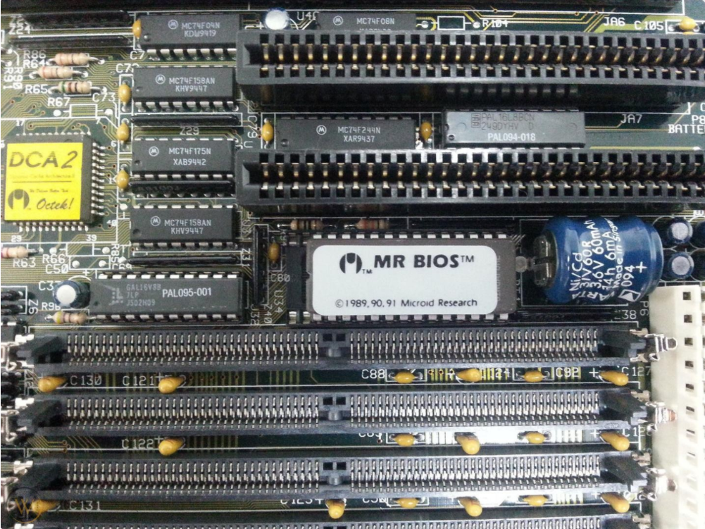
Hippo DCA2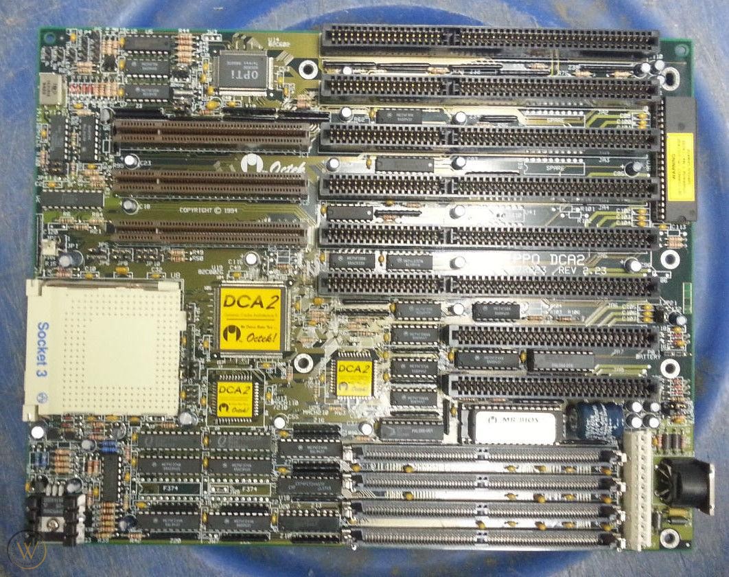 / DCA2-486 VLB / DCA2-486 VLB
Year: 1994
Type: Socket 3
Form Factor: Baby AT
Power Connector: AT
Chipset: OPTi 82C802G
BIOS: MR (Microid Research)
Slots: 6 x 16-bit ISA, 3 x VESA Local Bus
Memory: 4 x 30-pin SIMM
Known Board Revisions: 2.23
BIOS Strings:
More Images
|
Hippo 15 / Hippo-15
Year: 199x
Form Factor: Baby AT (8.5" x 12")
Power Connector: AT
Chipset: UMC 8881/8886 486 PCI
BIOS: Award (1 MB flash PnP)
Slots: 16-bit ISA x 4, PCI x 3
Memory: 4 x 72-pin FPM SIMM (256 MB max.)
Known Board Revisions: 1.2x
BIOS Strings:
Supports Intel 486DX/DX2/DX4 up to 100 MHz and OverDrive CPUs, AMD 486DX/DX2/DX4 up to 120 MHz, AMD X-5 5x86 133 MHz, Cyrix/TI 486DX/DX2/DX4 up to 100 MHz, and Cyrix 5x86 100 and 120 MHz.
FSB speeds of 25, 33, 40, and 50 MHz.
L2 cache is 256 KB as standard but also supports 0 KB, 64 KB, 128 KB and 512 KB.
Onboard EIDE via the UMC 8004 PCI EIDE chipset supports DMA Mode 2 (22 MB/sec) and PIO Modes 3 and 4 (17 MB/sec).
Jumper Settings
CPU Type
TYPE      JP1 JP2 JP10 JP11 JP13 JP14 JP15 JP16 JP17 JP18 JP21 JP22 JP23 JP24 JP25
-----------------------------------------------------------------------------------
Intel     1-2 1-2 open open 3-4  1-2  open open open 1-2  open open open open open
486DX/DX2                        3-4
Intel 	   1-2 1-2 open open open 2-3  open open open 1-2  open open open open open
486SX
Intel 	   1-2 1-2 2-3  1-2  2-3  1-2  open 2-3  1-2  3-4  2-3  2-3  open open open
P24T               4-5            3-4                 5-6
Cyrix 	  1-2 2-3 1-2  2-3  open 2-3  open 1-2  2-3  3-4  2-3  1-2  open open open
CX486S           3-4
Cyrix 	  1-2 2-3 1-2  2-3  3-4  1-2  open 1-2  2-3  3-4  2-3  1-2  open open open
CX486DX          3-4            3-4
UMC-U5S  2-3 1-2 open 3-4  1-2  2-3  open open open 1-2  1-2  open open open open
                           3-4
Intel 	  1-2 1-2 2-3  open open 2-3  open open open 3-4  2-3  2-3  open open open
SL 486SX         4-5
Intel SL 1-2 1-2 2-3  open 3-4  1-2  open open open 3-4  2-3  2-3  open open open
DX/DX2/DX4       4-5            3-4
AM486DXL 2-3 1-2 open 3-4  1-2  1-2  open open open 1-2  1-2  open open open open
AM486DX4                   3-4  3-4
UMC-U5DS
AM486DX2 1-2 1-2 2-3  open 3-4  1-2  2-3  open open 3-4  2-3  2-3  open open 1-2	.
AM486DX4         4-5            3-4
Intel    1-2 1-2 2-3  open 3-4  1-2  2-3  open open 3-4  2-3  2-3  1-2  1-2  1-2
P24D             4-5            3-4
AM486DX2 2-3 1-2 open 3-4  1-2  1-2  1-2  open open 1-2  1-2  open open open open
                           3-4  3-4
Cyrix    1-2 1-2 2-3  open 3-4  1-2  open open open 3-4  2-3  2-3  open 1-2  1-2
5X86             4-5            3-4
AMD      1-2 1-2 2-3  open 3-4  1-2  2-3  open open 3-4  2-3  2-3  1-2  1-2  1-2
5X86-133         4-5            3-4
Remark:
   To support AMD 5X86-133 CPU:     JP26 = OPEN, JP19 = 2-3
   To support Cyrix 5x86-100 CPU:   JP26 = OPEN, JP28=1-2,3-4,5-6, JP19 = OPEN
   To support Cyrix 5x86-120 CPU:   JP26 = OPEN, JP28=3-4,5-6, JP19 = OPEN
CPU Clock Multiple
JP19	Intel 486DX4  AMD Enhance 486DX4  AM 5x86
--------------------------------------------------------------------------------
open	 3x           3x                   n/a
1-2	 2.5x         n/a                  n/a
2-3	 2x           2x                   4x

Clock Selection
JP28            Clock Rate      CPU speed
--------------------------------------------------------------------------------
1-2             50MHz           DX50
1-2,3-4,5-6     33MHz           DX33, DX2-66, DX4-100
3-4,5-6         40MHz           DX40, DX2-80, DX4-120
5-6             25MHz           DX25, DX2-50, DX4-75

CPU Voltage
TYPE    CPU VCC        JP3	    JP4	    JP6
--------------------------------------------------------------------------------
AUTO	 5V/3.45V       1-2	    open 	open
FIXED	 5V             open	1-2 	open
FIXED	 3.6V           open	open 	1-2
FIXED	 3.45V          open	open 	open
Cache Configuration
For 33MHz clock, the tag RAM 32Kx8 is used 20ns, and 40MHz or 50MHz system, 15ns RAM is used (U2).
       512K            256K            256K            128K
       128Kx8          32Kx8           64Kx8           32Kx8
       U7-u10          U7-U10,U3-U6    U7-U10          U7-U10
   -------------------------------------------------------------------------------
JP9	2-3             1-2             2-3             2-3
JP12	1-2,3-4         1-2             1-2             open
User Manual |
Rhino 5
Year: 1995
Type: Socket 7
Form Factor: Baby AT (8.5" x 12.5")
Power Connector: AT
Chipset: OPTi Viper-M
BIOS: Award (1 MB flash PnP)
Slots: 4 x 16-bit ISA, 4 x PCI (Bus Mastering and fully PCI 2.0-compliant)
Memory: 4 x 72-pin SIMM (EDO or FPM supported, max. 128 MB)
Known Board Revisions:
BIOS Strings:
The Rhino 5 is a socket 7 board that supports Pentium 75/90/100/120/133/150/166/180 and 200 MHz. Also supported are the Cyrix 6x86 120+/150+/166+ CPUs.
FSB speeds of 50, 60 and 66 MHz. L2 cache can be either 256 KB or 512 KB.
Onboard memory can be 4 MB, 8 MB, 16 MB or 32 MB FPM or EDO modules.
EIDE interface supports PIO Modes 3 and 4 (17 MB/sec) and DMA Mode 2 (22 MB/sec). |
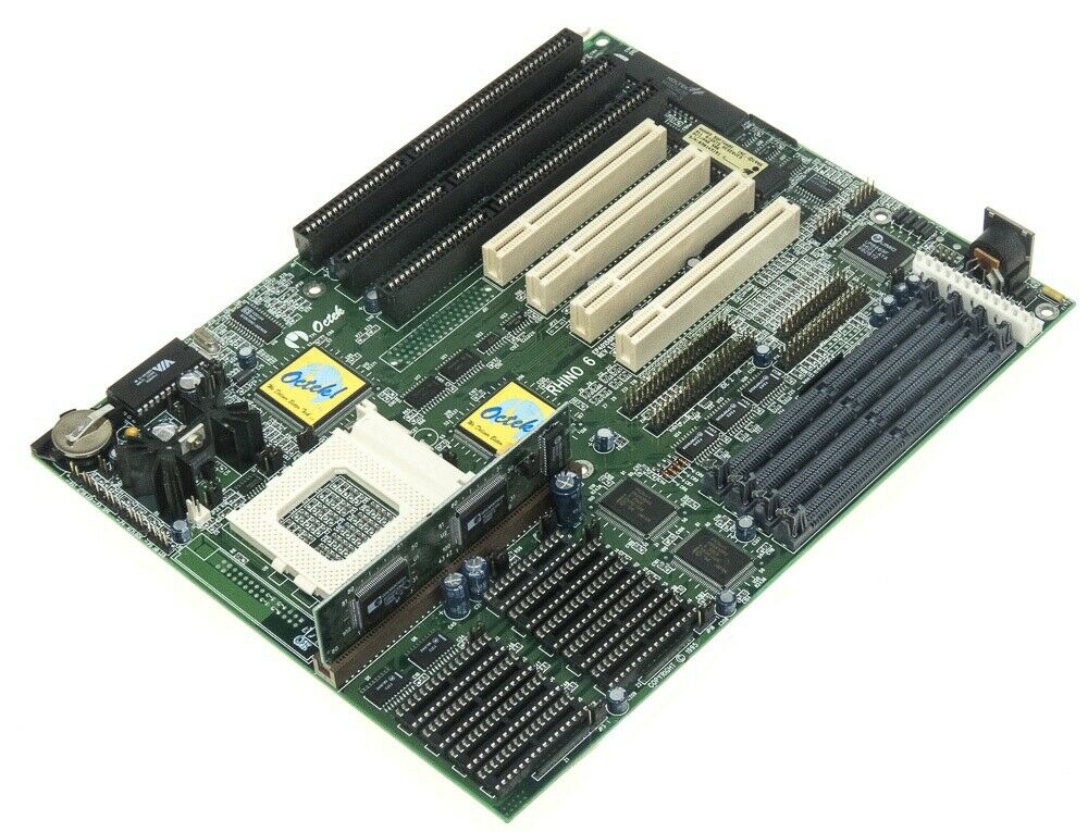
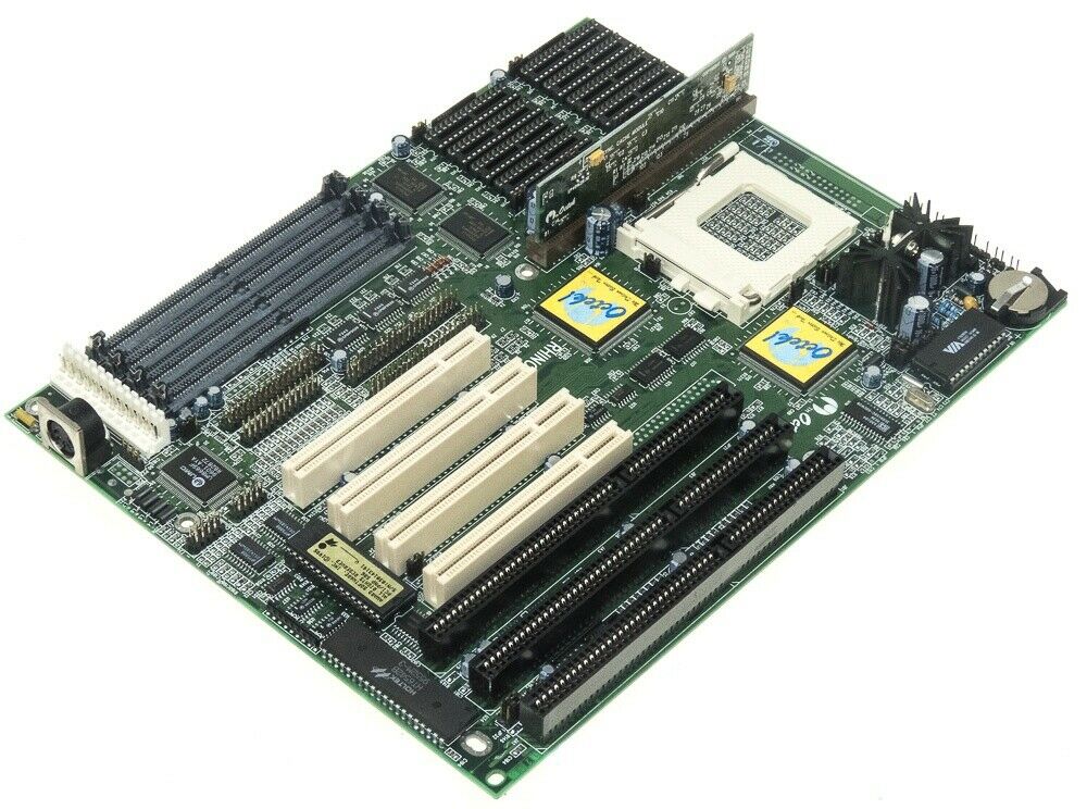
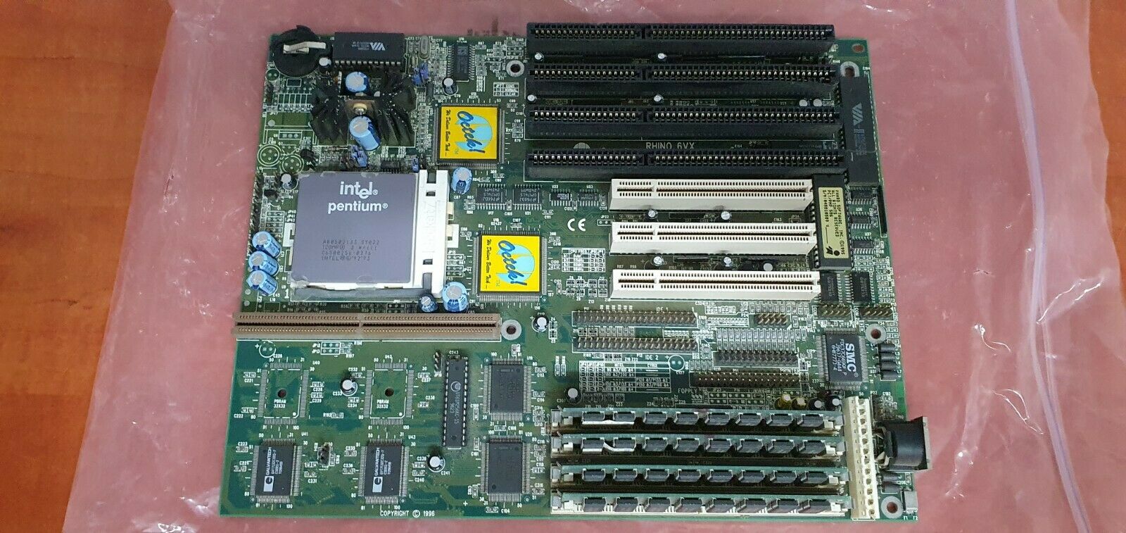
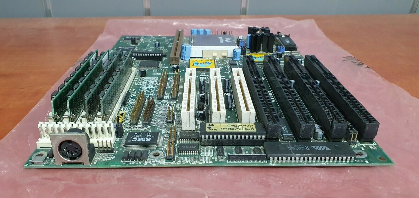
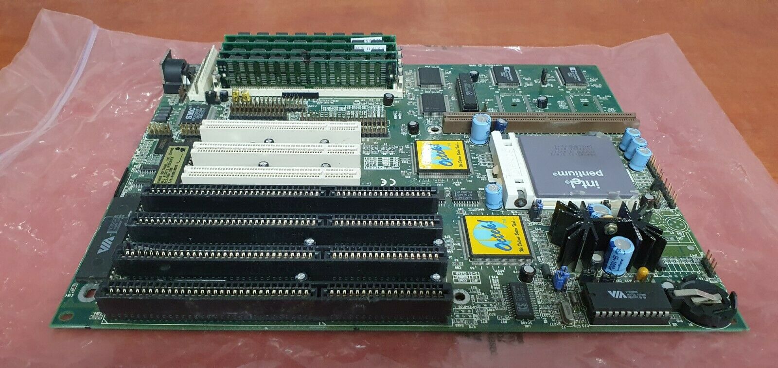
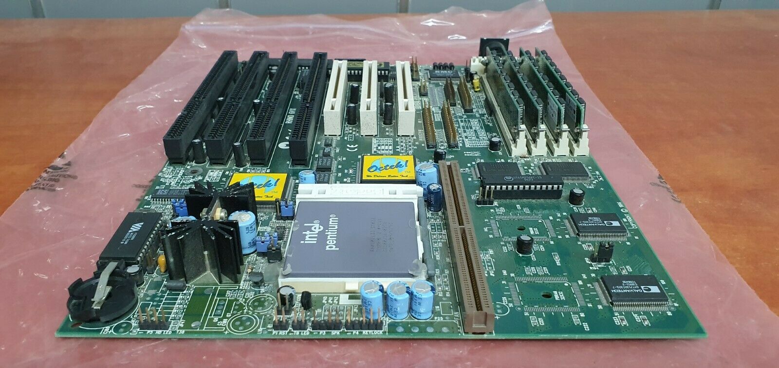
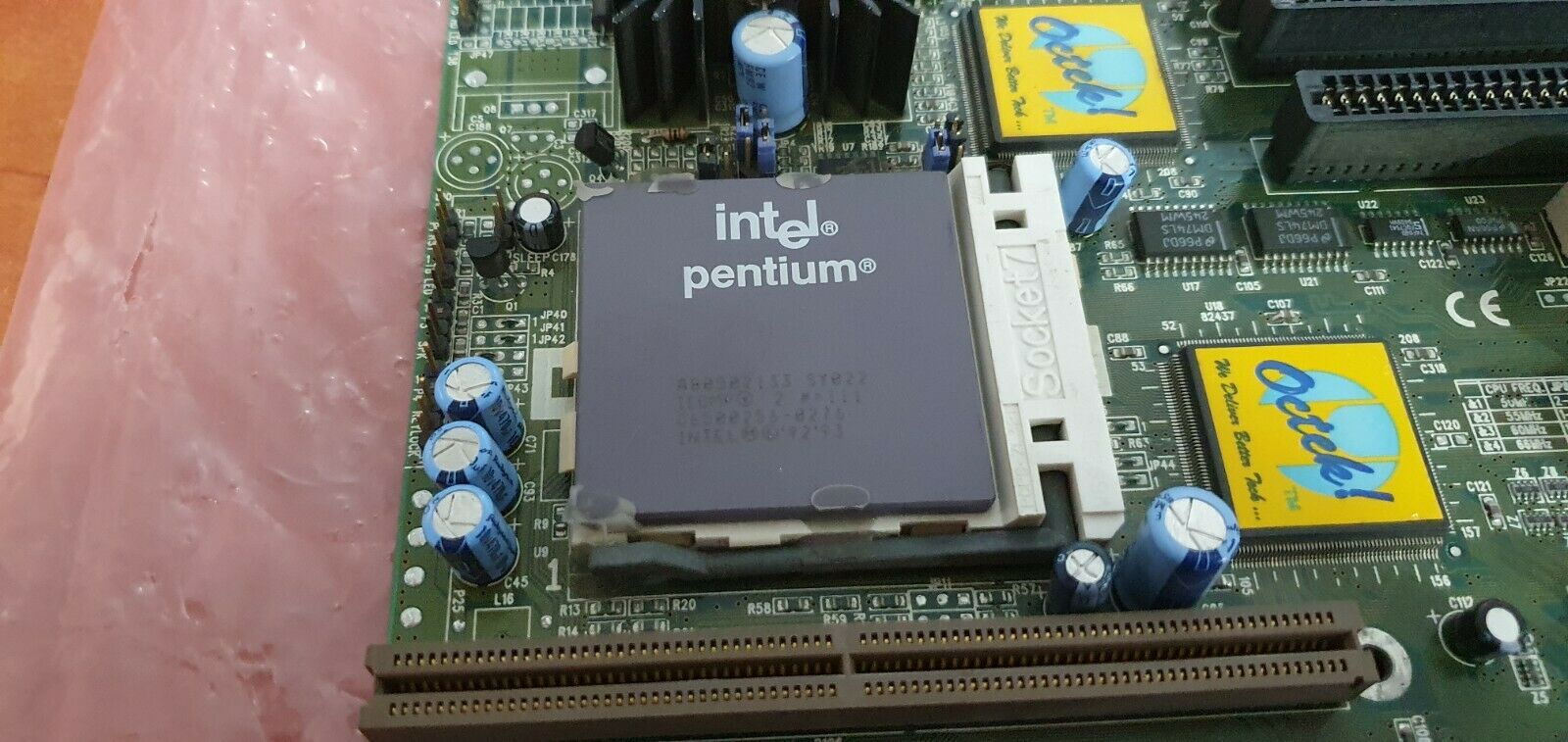
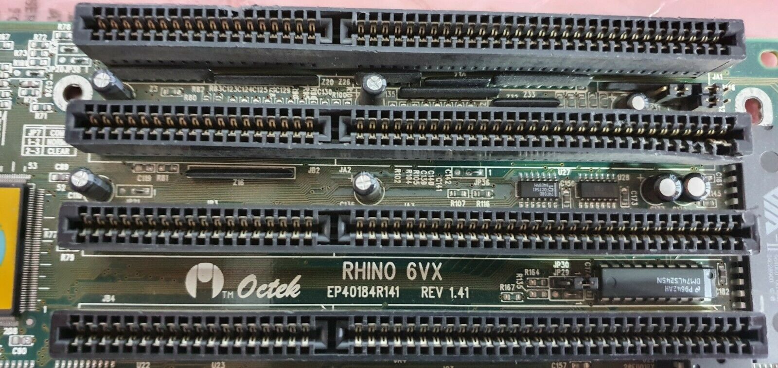
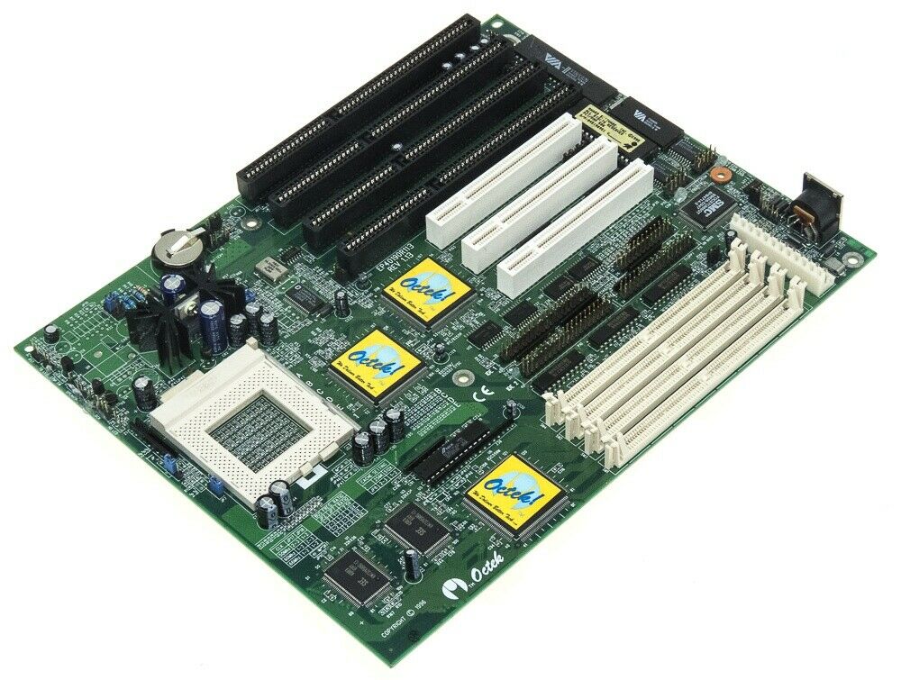
Rhino 6 / 6VX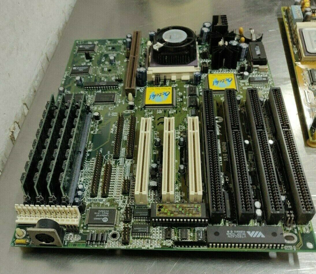
Year: 1995
Type: Socket 7
Form Factor: Baby AT (8.5" x 11")
Power Connector: AT
Chipset: Intel 430FX Triton (Rhino 6), 430VX (Rhino 6VX)
BIOS: Award (1 MB flash PnP)
Slots: 3 x 16-bit ISA, 4 x PCI (Rhino 6), 4 x 16-bit ISA, 3 x PCI (Rhino 6VX)
Memory: 4 x 72-pin SIMM (128 MB max.), COAST slot for cache
Known Board Revisions: 1.01 and 1.11 (Rhino 6), 1.2 and 1.41 (6VX)
BIOS Strings:
The Rhino is a socket 7 board that supports Pentium 75/90/100/120/133/150/166/180 and 200 MHz. Also supported are the Cyrix 6x86 120+/150+/166+ CPUs. In addition, the 6VX only also supports the AMD 5k86 series.
FSB speeds of 50, 60 and 66 MHz. L2 cache can be either 256 KB or 512 KB.
Onboard memory can be 4 MB, 8 MB, 16 MB or 32 MB FPM or EDO modules.
EIDE interface supports PIO Modes 3 and 4 (17 MB/sec) and DMA Mode 2 (22 MB/sec).
Jumper Settings:
CPU Type (CPU/L2 Cache BUS Speed) Settings
TYPE                         CPU Clock       JP8     JP9     JP10
--------------------------------------------------------------------------------
Intel P54C-75                50Mhz           2-3     2-3     1-2
Cyrix 6x86-P120+ (100Mhz)    50Mhz           2-3     2-3     1-2
AMD 5K86-P75 (75Mhz)         50Mhz           2-3     2-3     1-2
Intel P54C-90                60Mhz           1-2     2-3     2-3
Intel P54C-120               60Mhz           1-2     2-3     2-3
Intel P54CS-150              60Mhz           1-2     2-3     2-3
Intel P54C-180               60Mhz           1-2     2-3     2-3
Cyrix 6x86-P150+ (120Mhz)    60Mhz           1-2     2-3     2-3
AMD 5K86-P90 (90Mhz)         60Mhz           1-2     2-3     2-3
Intel P54C-100               66MHz           2-3     1-2     2-3
Intel P54C-133               66Mhz           2-3     1-2     2-3
Intel P54CS-166              66Mhz           2-3     1-2     2-3
Intel P54CS-200              66Mhz           2-3     1-2     2-3
Cyrix 6x86-133 (P166+)       66Mhz           2-3     1-2     2-3
AMD 5K86-P100 (100Mhz)       66Mhz           2-3     1-2     2-3

Clock Multiplier
                P54C            P54CS           P54CS           P55C
JP4     JP5     P54CQS          B-STEP          C-STEP
--------------------------------------------------------------------------------
2-3     2-3     reserved        reserved        x2.5            x2.5
1-2     2-3     reserved        reserved        reserved        reserved
2-3     1-2     x2              x2              x2              x2
1-2     1-2     x1.5            x1.5            x1.5            reserved

Multiplier selection based on CPU type
TYPE                         JP4     JP5
--------------------------------------------------------------------------------
Intel P54C-75                1-2     1-2
Intel P54C-90                1-2     1-2
Intel P54C-100               1-2     1-2
Intel P54C-120               2-3     1-2
Intel P54C-133               2-3     1-2
Intel P54C-150               2-3     2-3
Intel P54C-166               2-3     2-3
Intel P54C-180               1-2     2-3
Intel P54C-200               1-2     2-3
Cyrix 6x86-100 (P120+)       2-3     1-2
Cyrix 6x86-120 (P150+)       2-3     1-2
Cyrix 6x86-166 (P133+)       2-3     1-2
AMD 5K86-P75 (75Mhz)         1-2     1-2
AMD 5K86-P90 (90Mhz)         1-2     1-2
AMD 5K86-P100(100Mhz)        2-3     1-2

External Cache (L2 cache) setting
Async Cache / Sync Cache size selection
TYPE                    JP11
--------------------------------------------------------------------------------
256k                    2-3
512k                    open
0k                      open

Async Cache / Sync Cache size
TYPE           JP13     JP12    JP16
--------------------------------------------------------------------------------
0K              1-2     1-2     1-2
256KB           1-2     2-3     1-2
512KB           2-3     1-2     2-3

Voltage Source for Asynchronous L2 Cache
Note : Theses Jumpers are for Async On-board Cache only and have no effect on COAST Modules
TYPE            JP2     JP3     JP17    JP18
--------------------------------------------------------------------------------
+5V supply      2-3     2-3     2-3     2-3
+3.3V supply    1-2     1-2     1-2     1-2


Peripheral Setup
PS/2 Mouse support
TYPE            JP31    JP32    JP33
--------------------------------------------------------------------------------
Enabled         1-2     2-3     2-3
Disabled        2-3     1-2     1-2

Printer Port Interrupt
TYPE            JP25
--------------------------------------------------------------------------------
IRQ5            1-2
IRQ7            2-3
More Images (RHINO 6)
More Images (RHINO 6VX)
|
Rhino 8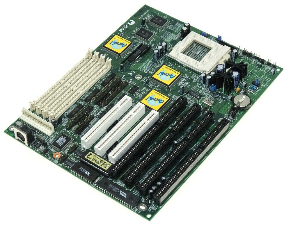
Year: 1996
Type: Socket 7
Form Factor: Baby AT
Power Connector: AT
Chipset: OPTi Viper-M
BIOS: Award
Slots: 4 x 16-bit ISA, 3 x PCI
Memory: 4 x 72-pin SIMM
Known Board Revisions: 1.13
BIOS Strings:
07/08/96-i430HX-U8669-2A59FO09C-00
The Rhino 8 is a socket 7 board that supports Pentium P54C CPUs.(?)
More Images
|
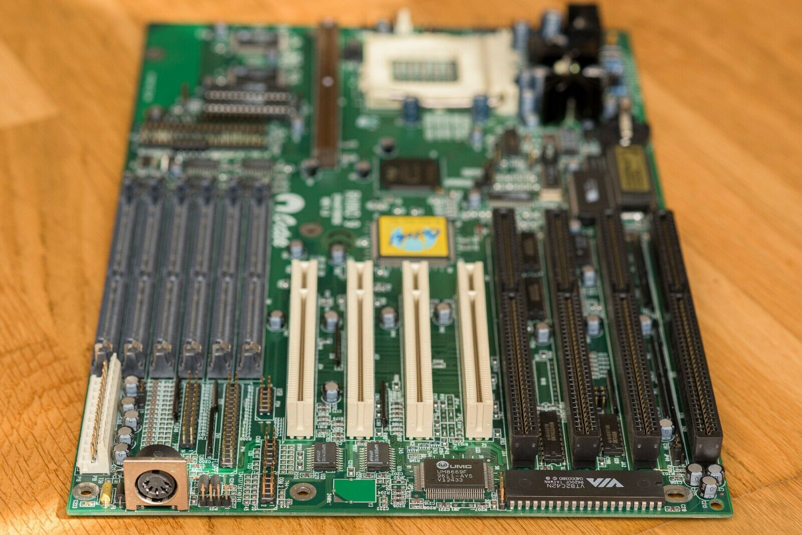
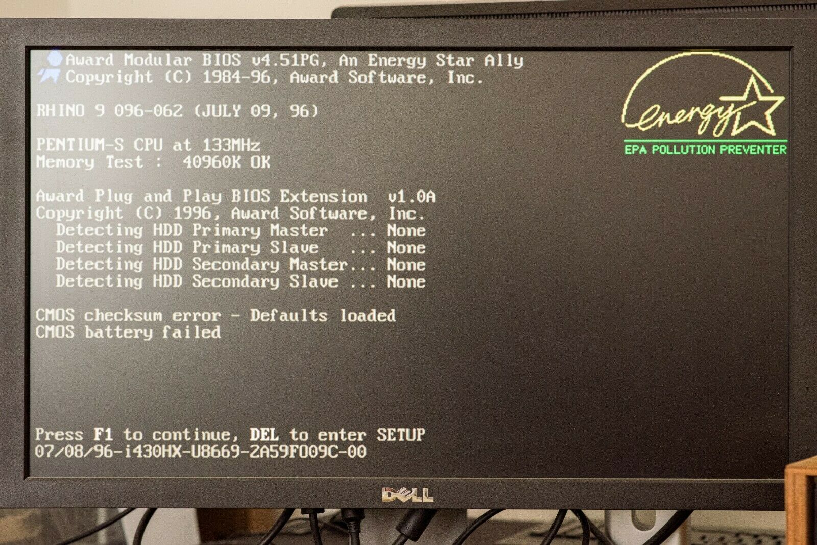
Rhino 9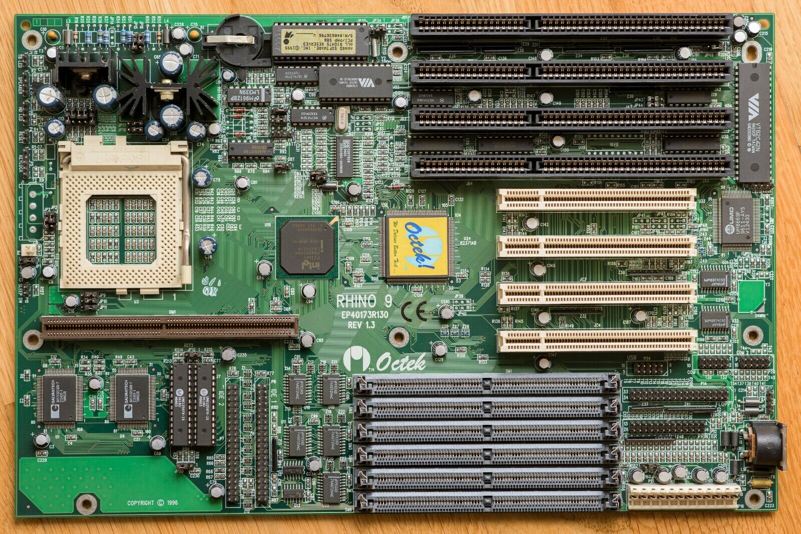
Year: 1996
Type: Socket 7
Form Factor: Baby AT (8.5" x 13")
Power Connector: AT
Chipset: Intel 430HX (Triton II)
BIOS: Award (1 MB flash PnP)
Slots: 4 x 16-bit ISA, 4 x PCI (fully PCI 2.1 compliant)
Memory: 6 x 72-pin FPM or EDO SIMM (384 MB max.), COAST 2.0 slot for cache
Known Board Revisions: 1.12, 1.3, 1.4
BIOS Strings:
07/08/96-i430HX-U8669-2A59FO09C-00
The Rhino 9 is a socket 7 board that supports Pentium 75/90/100/120/133/150/166/180 and 200 MHz. Also supported are the Cyrix 6x86 120+/150+/166+ CPUs and the AMD 5k86 series.
Pentium P55C (MMX) CPUs also supported on board revisions v1.3 and later.
Onboard dual-voltage jumpers.
FSB speeds of 50, 60 and 66 MHz. L2 cache can be either 256 KB or 512 KB.
Onboard memory can be 4 MB, 8 MB, 16 MB, 32 MB or 64 MB FPM or EDO modules.
EIDE interface supports PIO Modes 3 and 4 (17 MB/sec) and DMA Mode 2 (22 MB/sec).
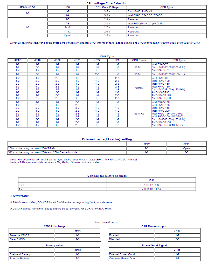
Jumper Settings
CPU Voltage Core Selection
For Rhino-9 rev 1.1x:
CPU Type                          CPU Core Voltage      JP16
----------------------------------------------------------------------------------
Intel P54C, P54CQS or                   3.3V            1-2
Intel P54CS, 54CTB, or
AMD 5k86 P75-P100
Cyrix 6x86 Full Spec/C-Spec(028) 3.5V open
Note: Rhino 9 v1.1x does not support MMX processor
For Rhino-9 rev 1.3:
CPU Type               CPU Core Voltage    JP9   JP10   JP11   JP15    JP17   JP18
----------------------------------------------------------------------------------------
Intel P55C CPU(MMX)        2.8V            2-3    2-3    2-3    2-3    2-3    2-3
Intel P54C, P54CQS or      3.5V(VRE)       1-2    1-2    1-2    2-3    1-2    1-2
Intel P54CS, 54CTB, or
Cyrix 6x86 or
AMD 5k86 P75-P100
For Rhino-9 rev 1.4x:
CPU Core Voltage    JP9   JP10   JP11   JP17   JP18   JP52         CPU TYPE
--------------------------------------------------------------------------------------
2.5V                2-3    2-3    2-3    2-3    2-3    open        For future CPU
2.8V                2-3    2-3    2-3    2-3    2-3    1-2         Intel P55C CPU(MMX)
2.9V                2-3    2-3    2-3    2-3    2-3    3-4         For future CPU
3.3V                1-2    1-2    1-2    1-2    1-2    5-6         Intel P54C, P54CQS or

Intel P54CS, 54CTB, or
AMD k5-PR75, PR90
3.5V(VRE)           1-2    1-2    1-2    1-2    1-2    7-8         Cyrix 6x86 CPU or
AMD K5-PR100
Note: Be careful to select the appropriate Core voltage for different CPU.
Improper Core voltage supplied to CPU may result in  "PERMENENT DAMAGE" to CPU!
CPU Type (CPU/L2 Cache BUS Speed) Settings
TYPE                      CPU Clock    JP28      JP29      JP8      JP25      JP2       JP3
--------------------------------------------------------------------------------------------
Intel P54C-75               50MHz       2-3       2-3       1-2      1-2      1-2       1-2
Cyrix 6x86-P120+(100Mhz)    50MHz       2-3       2-3       1-2      1-2      2-3       1-2
AMD 5k86-P75(75Mhz)         50MHz       2-3       2-3       1-2      1-2      1-2       1-2
Intel P54C-90               60MHz       1-2       2-3       1-2      2-3      1-2       1-2
Intel P54C-120              60MHz       1-2       2-3       1-2      2-3      2-3       1-2
Intel P54C-150              60MHz       1-2       2-3       1-2      2-3      2-3       2-3
Intel P54C-180              60MHz       1-2       2-3       1-2      2-3      1-2       2-3
Cyrix 6x86-P150+(120Mhz)    60MHz       1-2       2-3       1-2      2-3      2-3       1-2
AMD 5k86-P90                60MHz       1-2       2-3       1-2      2-3      1-2       1-2
AMD 5k86-P120(90Mhz)        60MHz       1-2       2-3       1-2      2-3      1-2       1-2
Intel P54C-100              66Mhz       2-3       1-2       2-3      2-3      1-2       1-2
Intel P54C-133              66Mhz       2-3       1-2       2-3      2-3      2-3       1-2
Intel P54C-166              66Mhz       2-3       1-2       2-3      2-3      2-3       2-3
Intel P54C-200              66Mhz       2-3       1-2       2-3      2-3      1-2       2-3
Intel P55C-166(MXX-166)     66Mhz       2-3       1-2       2-3      2-3      2-3       2-3
Intel P55C-200(MMX-200)     66Mhz       2-3       1-2       2-3      2-3      1-2       2-3
Cyrix 6x86-P166(133Mhz)     66Mhz       2-3       1-2       2-3      2-3      2-3       1-2
AMD 5k86-P100               66Mhz       2-3       1-2       2-3      2-3      1-2       1-2
AMD 5k86-P133(100Mhz)       66Mhz       2-3       1-2       2-3      2-3      1-2       1-2

External Cache(L2 cache) setting
Async Cache/ Syn Cache Size
For Rhino-9 rev 1.12, require Sync. Cache Module EP40178R101 Ver C Octek rev.101 w/o Tag Ram
Total Cache Size      JP4       JP5       JP6       JP7       JP12
---------------------------------------------------------------------------------------
0KB                   1-2       1-2       1-2       1-2       1-2
256KB                 2-3       1-2       1-2       1-2       1-2
512KB                 1-2       2-3       2-3       2-3       2-3
For Rhino-9 rev 1.3, 1.4, require Sync. Cache Module EP40178R300 Ver C Coast 3.0 w/o Tag Ram*
Total Cache Size      JP4       JP5       JP6       JP7       JP12      JP1*
---------------------------------------------------------------------------------------
0KB                   1-2       1-2       1-2       1-2       1-2
256KB                 2-3       1-2       1-2       1-2       1-2
512KB                 open      open      open      open      2-3       2-3

CPU Fan Voltage Select
                    JP1(Rhino-9 rev 1.12, 1.4)	JP35(Rhino-9 rev 1.3)
---------------------------------------------------------------------------------------
+5V                 1-2                              1-2
+12V                2-3                              2-3

Peripheral Setup
PS/2 Mouse support
                     JP49      JP43      JP44
---------------------------------------------------------------------------------------
Enabled              1-2       2-3       2-3
Disabled             2-3       1-2       1-2
Miscellaneous
Power Good Signal Select
                           JP42
---------------------------------------------------------------------------------------
External Power Good        1-2
On-board Power Good        2-3

CMOS discharge
                            JP21
-------------------------------------------------------------------------------------
Preserve CMOS              1-2
Clear CMOS                 2-3
Battery Select
                           JP23
-------------------------------------------------------------------------------------
On-board Battery           1-2
External Battery           2-3
More Images
    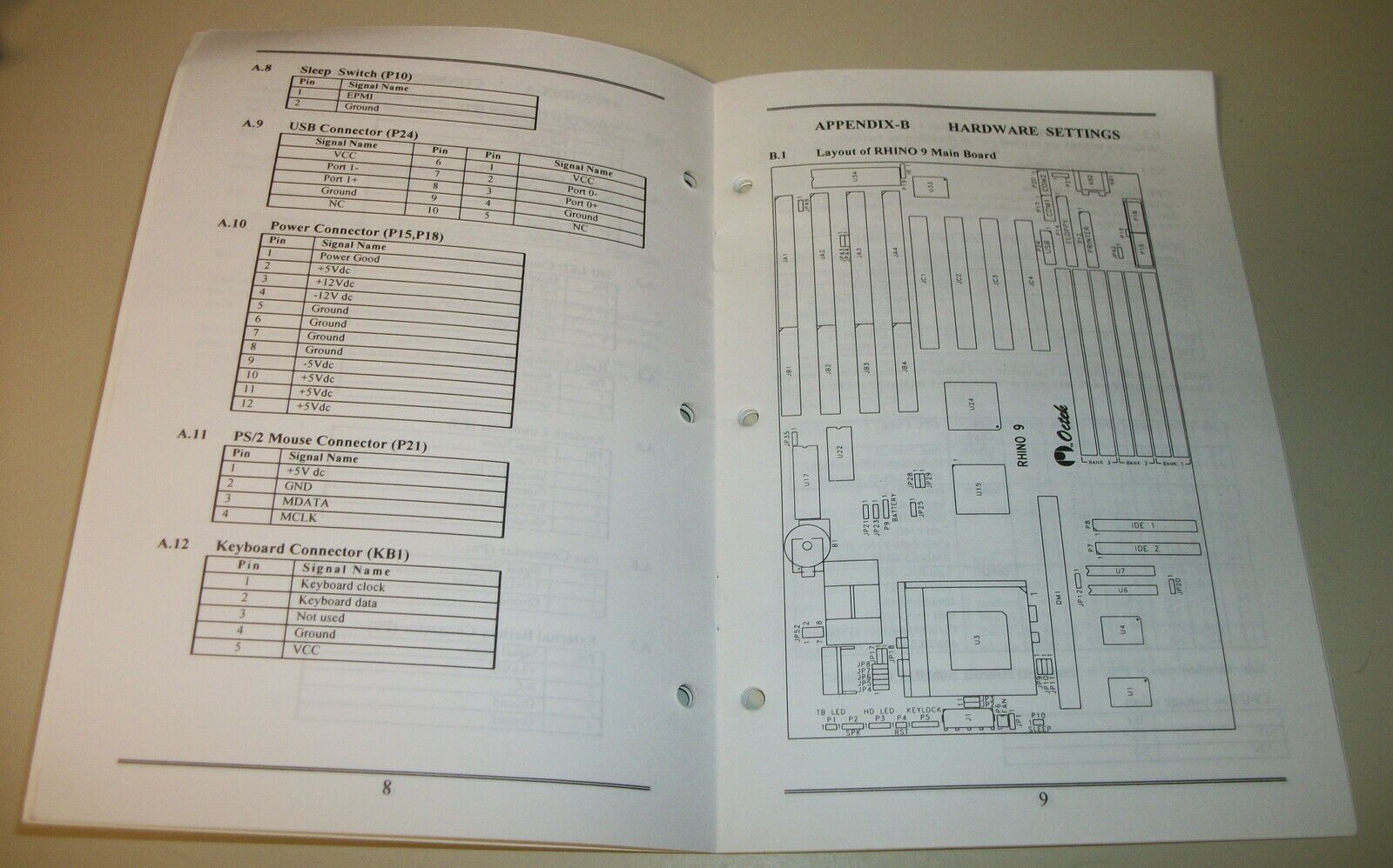
|
Rhino 10
Year: 199?
Type: Socket 7
Form Factor: Baby AT
Power Connector: AT
Chipset: Intel 430VX
BIOS: Award PnP Green
Slots: 4 x 16-bit ISA, 3 x PCI
Memory: 4 x 72-pin SIMM (FPM, EDO, SDRAM) and 2 x 168-pin DIMM (128 MB max.), COAST slot for cache
Known Board Revisions: 1.03, 1.05
BIOS Strings:
The Rhino 10 is a socket 7 board that supports Pentium 75/90/100/120/133/150/166/180 and 200 MHz, in addition to Intel Pentium MMX CPUs. Also supported are the AMD 5k86 P75-P133 and Cyrix 6x86 P120+/P150+/P166+ CPUs.
The 72-pin memory slots can use 4 MB, 8 MB, 16 MB, 32 MB with a mix of Fast Page Mode (FPM), EDO DRAM, and SDRAM.
Jumper Settings
|
Rhino II LX-ATX
Year: 199x
Type: Slot 1
Form Factor: AT
Power Connector: AT and ATX
Chipset: Intel 440LX (Balboa)
BIOS: Award v4.51PG
Slots: 3 x 16-bit ISA, 3 x PCI, 1 x AGP
Memory: 2 x 168-pin DIMM (PC100)
Known Board Revisions:
BIOS Strings:
Rhino II LX-AT supports Pentium II CPUs up to 333 MHz in a Slot 1 package. The FSB can be run at up to 100 MHz.
It comes with 2 USB ports, an onboard EIDE hard disk and floppy controller interface.
A Socket 370 variant of the Rhino II LX-ATX also exists, which support later Pentium II CPUs as well as Intel Celeron CPUs up to 450 MHz. |
Rhino II BX-ATX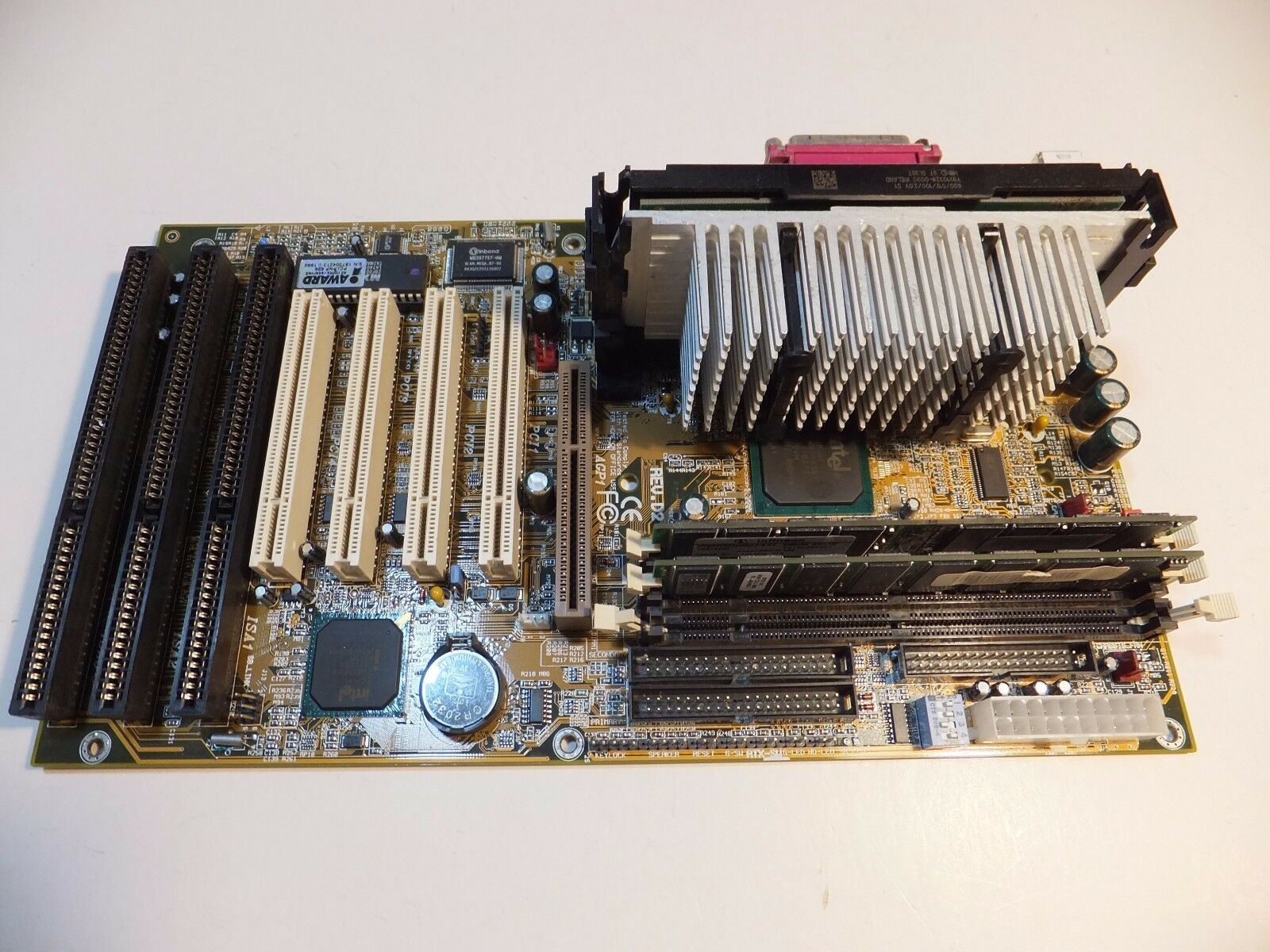
Year: 199x
Type: Slot 1
Form Factor: ATX
Power Connector: AT
Chipset: Intel 440BX (Seattle)
BIOS: Award v4.51PG
Slots: 3 x 16-bit ISA, 4 x PCI, 1 x AGP
Memory: 3 x 168-pin DIMM (PC100)
Known Board Revisions: D2
BIOS Strings:
10/26/99-i440BX-ED-2A69KD4FC-00
Rhino II BX-ATX supports Pentium II CPUs up to 500 MHz in a Slot 1 package. The FSB can be run at up to 100 MHz. The board also comes with USB sockets and a dual onboard EIDE hard disk controller.
It also was one of the earliest boards to come with built-in health monitoring.
A small footprint version of the II BX-ATX exists, called the II BX-SATX. This comes with 2 ISA slots and 3 PCI slots, but is otherwise the same. |
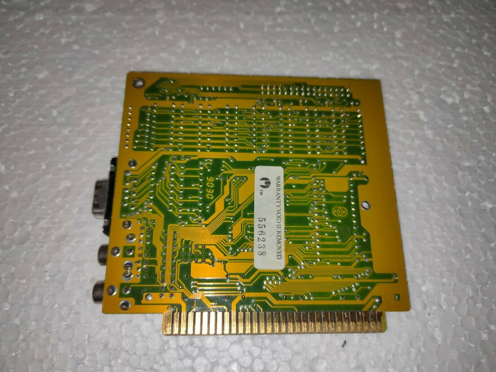
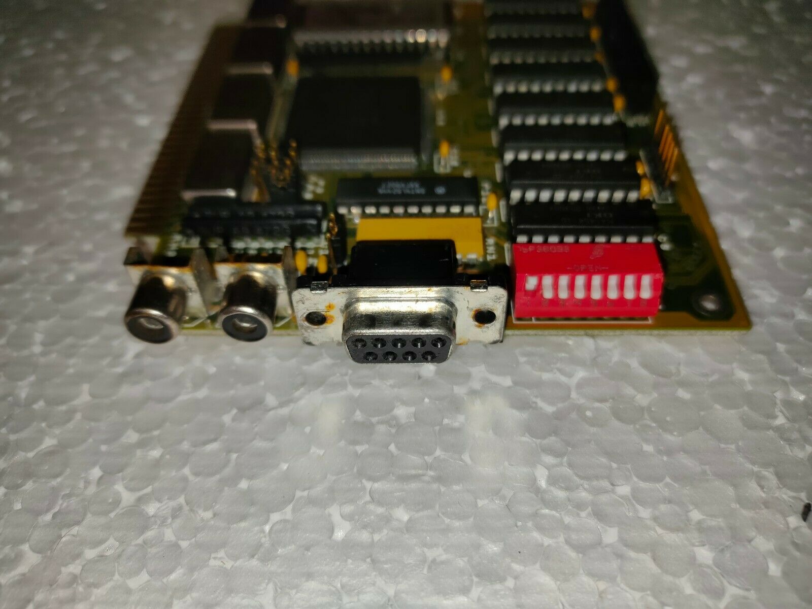
MicroEGA / VC-001
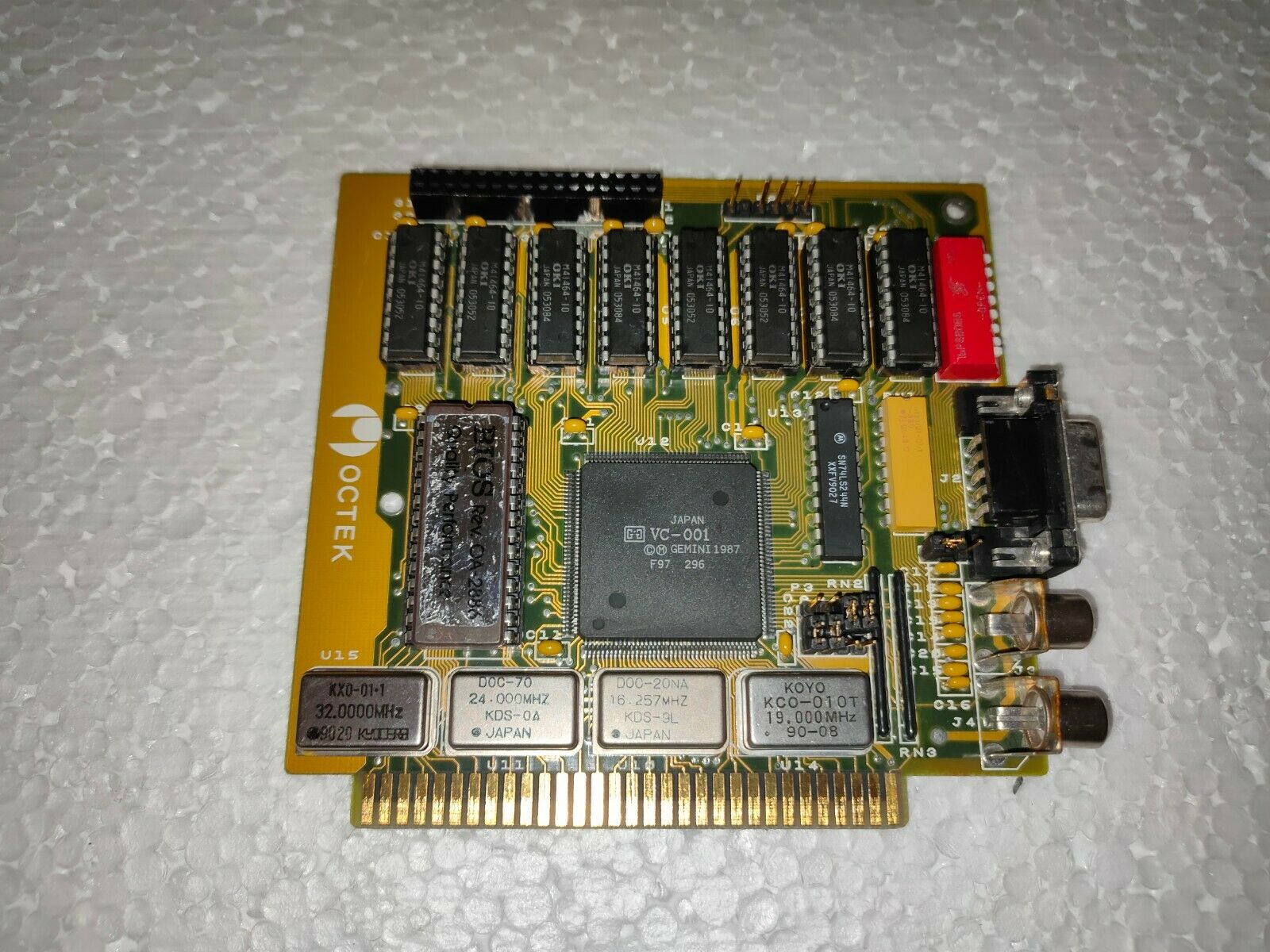 Launched: 1985 Launched: 1985
Bus: ISA 8-bit
Chipset: Gemini VC-001
Memory: 256 KB
Price: ?
FCC ID: -
The MicroEGA is an EGA card with 256 KB of video RAM onboard. The board is supposedly manufactured by Seiko.
It appears to also support composite and RGB out via the two RF output jacks on the edge connector.
I did a full 3-part review of the MicroEGA in May 2022.
More Images
|
.jpg) EVGA-8 EVGA-8
Launched: 1990
Chipset: Chips & Technologies 82C451
Bus: ISA 8-bit
Memory: 256 KB
RAMDAC: Samsung KDA0476CN
RAMDAC Speed: 50 MHz
Price: ?
Part #: 900143 (Rev.1) or EP2240-0003-<Rev> (Later Revisions)
FCC ID: -
Known Board Revisions: 1.0, 3.0
The EVGA-8 is a VGA-compatible card capable of displaying up to 256 colours via its 8-bit RAMDAC.
|
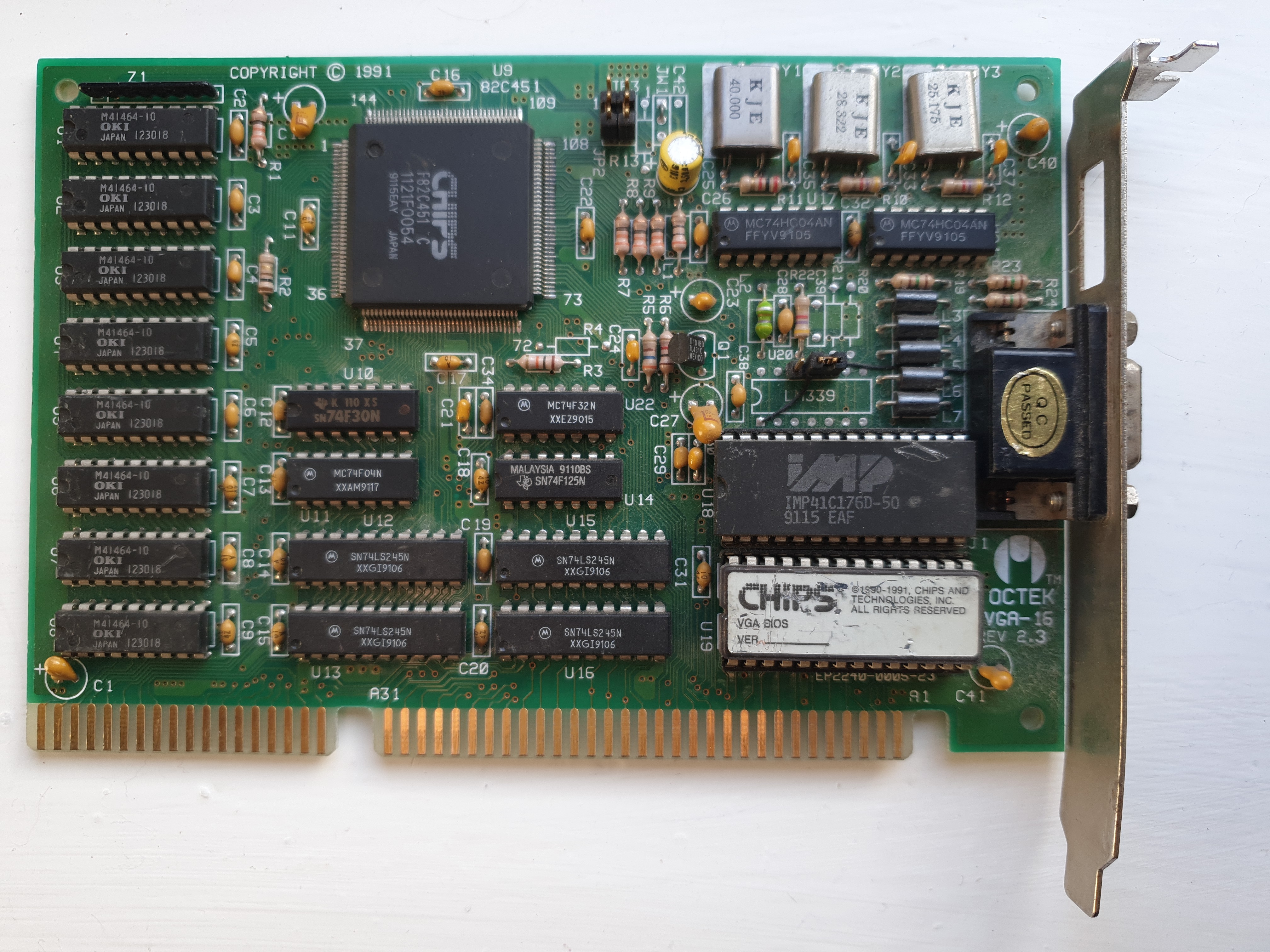
.jpg) EVGA-16 EVGA-16
Launched: 1991
Chipset: Chips & Technologies 82C451
Bus: ISA 16-bit
Memory: 256 KB
RAMDAC: IMP41C176D, Avasem AV3676 or Inmos IMSG171P
RAMDAC Speed: 50 MHz
Price: ?
Part #: EP2240-0005-<Rev>
FCC ID: -
Known Board Revisions: 2.0, 2.1, 2.3
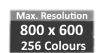
The EVGA-16 is the 16-bit ISA version of the earlier EVGA-8 card, and is functionally identical though performance is likely faster given the 16-bit bus access. It is an SVGA-compatible card capable of displaying up to 256 colours at a resolution of 320 x 320, or 16 colours at 800 x 600 via its 8-bit RAMDAC. It also supports 132-column text mode.
The memory is soldered-in on all these boards as there was no option to expand the memory beyond the 256 KB provided, since that is the maximum the chipset supports.
The C&T chipset supports Hercules, MDA, CGA and EGA modes as well, though the card doesn't output digital TTL signals so this is emulated for display on your analogue VGA monitor.
The VGA ROM BIOS is a single 64 KB EPROM chip.
This VGA card is known to work in an 8-bit ISA slot. More Images
.jpg)
|
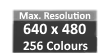
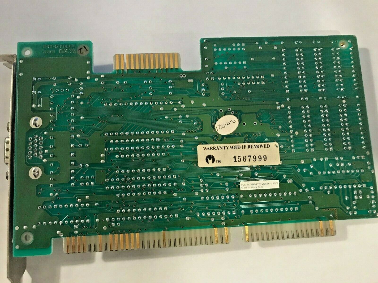
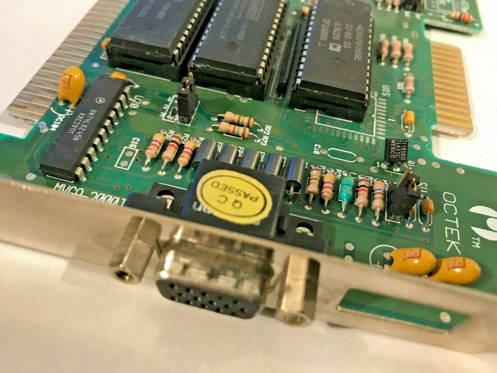
MVGA 2000-II
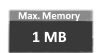 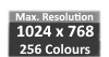
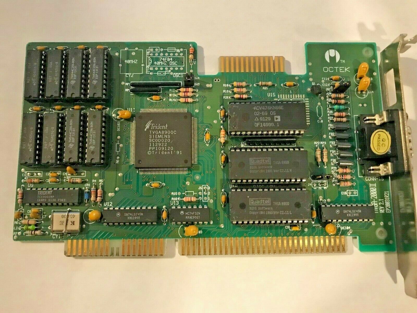 Launched: 1990 Launched: 1990
Chipset: Trident TVGA8900C
Bus: ISA 16-bit
Memory: 1 MB
Price: ?
FCC ID: HNG2YPTVGA96
This card is a super VGA card based around the ubiquitous Trident TVGA-8900C chipset.
More Images
|
PVGA1C
Launched: 1991
Chipset: Western Digital WD90C11A or IMP41C1760
Bus: ISA 16-bit
Memory: 256 KB or 512 KB DRAM
Memory Clock: 45 MHz
RAMDAC:
Music Semiconductor TR9C1710
RAMDAC Clock: 66 MHz
Price: ?
FCC ID: ?
Known Board Revisions: Rev.2 |
Trident 9680
Launched: 1996/1997?
Chipset: Trident TGUI9680
Bus: PCI
Memory: 1 MB DRAM (upgradable to 2 MB, EDO)
Dot Clock: -
RAMDAC: (Unknown) - supports HiColor and TrueColor
Price: ?
FCC ID:
The Trident 9680 was a 64-bit PCI video/GUI accelerator card launched around 1996. Its graphics coprocessor had hardware support for BitBLT, image & text transfer, Hardware cursor, line draw, short stroke vector draw, rectangle fills, Clipping, trapezoid fills and 256 ROPs (Raster Operations).
Other features of the TGUI9680 include:
- On-Chip Color Space Conversion(CSC)
- H/V scaling & overlay control for 30 FPS software video CODEC display
- Feature connector and VAFC(Optional)
- 64-Bit GUI engine
- Support linear addressing
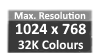
It supported resolutions of 1280x1024 in 16.7 million colours. At 1,024x768 it could manage refresh rates up to 75 Hz.
Video memory was 256Kx16 SOJ in 60ns or 70ns speeds, accessible via a 64-bit interface.
Drivers for Windows 3.x, Windows 95 OSR2, Windows NT 3.51, and OS/2 were provided. |
Macronix MX96250
Launched: 1996/1997?
Chipset: Macronix MX96250
Bus: PCI
Memory: 1 MB DRAM (upgradable to 2 MB, EDO)
RAMDAC: (Unknown) - supports TrueColor
RAMDAC Speed: 135 MHz
Price: ?
FCC ID:
The Macronix MX96250 card launched around 1996, and was a 64-bit graphics and video accelerator engine. On the video side, it could manage over 30 fps full-screen video playback for Indeo, Cinepak, and MPEG-1 CODECs.
The card's memory interface is 64-bit and supports fast page mode and hyper page EDO DRAMs via four pieces of 256Kx16 SOJ.
Drivers for Windows 3.x, Windows 95, Windows NT 3.51, and OS/2 were provided, in addition to a DCI (Display Control Interface) driver for Windows 3.x and 95 for video playback. |
Speed-64
 
Launched: 1997/1998?
Chipset: Ark Logic ARK2000
Bus: PCI
Memory: 1 MB DRAM (upgradable to 2 MB)
Dot Clock: 135 MHz
RAMDAC: Chrontel HiColor and TrueColor
Price: ?
FCC ID:
The Speed-64 was a 64-bit PCI graphics accelerator card launched around 1997. Its graphics coprocessor had hardware support for Bitblt, Rectangle Fill, Rectangle Clipping, Raster Operations, Line Draw, Pattern Fill, Color Expansion, Image Transfer, Draw and Step, and Transparency operations.
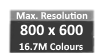
It supported resolutions of 1600x1200 in 256 colours (86 Hz interlaced), 1280x1024 in 64,000 colours up to 75 Hz refresh rate (non-interlaced) or 86 Hz (interlaced), and 800x600 in 16.7 million colours at up to 90 Hz (non-interlaced).
Video memory was 256Kx16 SOJ in 60ns or 70ns speeds, accessible via a 64-bit interface.
Drivers for Windows 3.x, Windows 95 OSR2, Windows NT 3.51, and OS/2 were provided. |
 Octek
Octek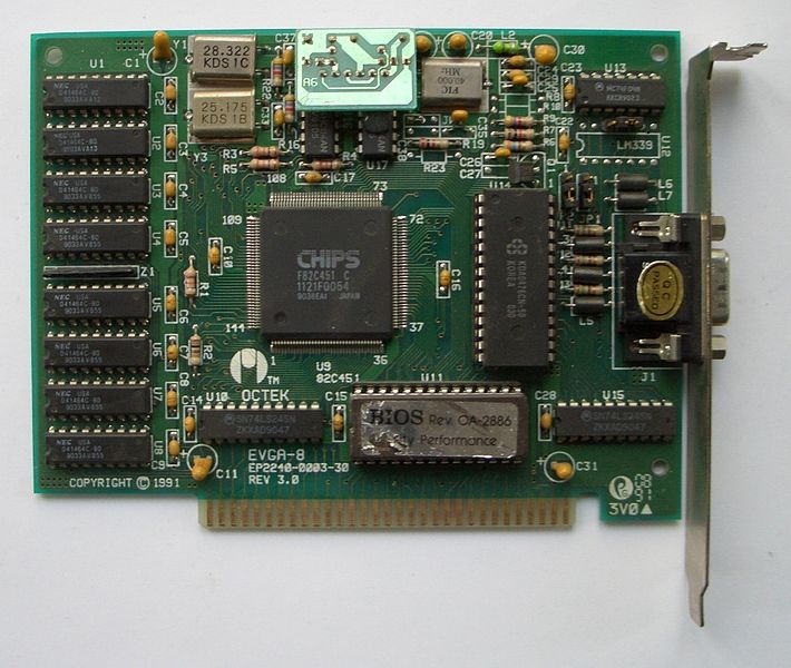